How Read Engine Codes 2002 Ultra Classic
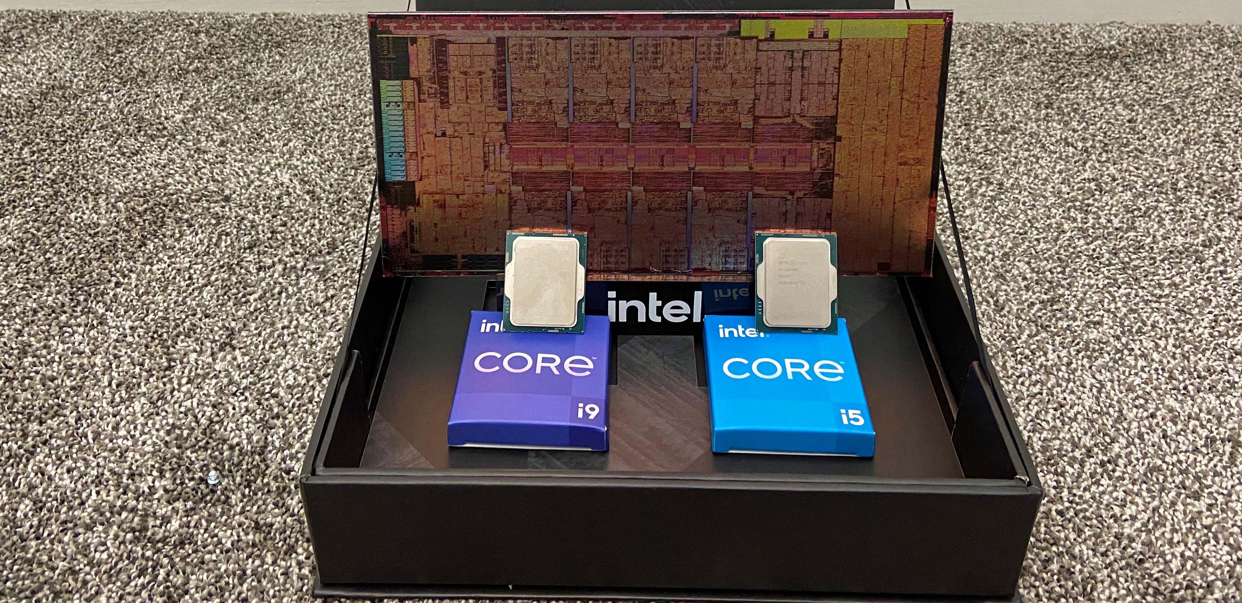
Intel 12th-Gen Alder Lake Pricing, Benchmarks, Specs and All Nosotros Know
Alder Lake has finally arrived to the market place and we at present accept our reviews of the leading-border Core i9-12900K, Core i7-12700K, and Core i5-12600K, and Core i5-12400 with all of the performance benchmarks and assay. Overall, the Core i5-12600K is now the Best CPU for gaming on the market, while the Core i7-12700K slots in equally the best high-end processor for mainstream platforms. Intel has also released a full lineup of 22 additional lower-priced desktop Alder Lake fries and a new lineup of Laminar coolers. Nosotros've also included our full performance benchmarks in the article below.
Intel's twelfth-Gen Alder Lake chips bring the visitor's hybrid compages, which combines a mix of larger loftier-performance cores paired with smaller high-efficiency cores, to desktop x86 PCs for the first time. Intel has already released the higher-finish models for the desktop PC, but the visitor has augmented those fries with the more mainstream models it recently launched. It also appears that Intel will besides add the new design to its lowest-cease fries, too. We also expect the Alder Lake models for laptops to also get in in January.
| Toll | Cores | Threads | P-Core Base/Heave | E-Core Base/Boost | TDP / PBP / MTP | DDR4-3200 | L3 Cache | |
| Core i9-12900K / KF | $589 (Thou) - $564 (KF) | 8P + 8E | xvi Cores / 24 Threads | 3.ii / v.2 GHz | ii.iv / 3.9 GHz | 125W / 241W | DDR4-3200 / DDR5-4800 | 30MB |
| Core i7-12700K / KF | $409 (K) - $384 (KF) | 8P + 4E | 12 Cores / twenty Threads | 3.six / 5.0 GHz | 2.7 / 3.8 GHz | 125W / 190W | DDR4-3200 / DDR5-4800 | 25MB |
| Core i5-12600K / KF | $289 (Yard) - $264 (KF) | 6P + 4E | 10 Cores / xvi Threads | 3.7 / iv.9 GHz | 2.8 / 3.6 GHz | 125W / 150W | DDR4-3200 / DDR5-4800 | 16MB |
| Cadre i5-12400 / F | Estimated ~ $185 - $160 | 6P + 0E | half dozen Cores / 12 Threads | 4.4 / ~2.5 GHz | north/a | 65W / 117W | DDR4-3200 / DDR5-4800 | 18MB |
Intel's initial Alder Lake lineup starts with 3 fries and their graphics-less variants, with the flagship $589 Cadre i9-12900K, which Intel bills equally the 'globe's fastest gaming processor,' leading the charge with 16 cores and 24 threads. Intel claims this chip provides an average 13% generational jump in gaming operation, beats AMD'south Ryzen 9 5950X flagship by upward to 30% in gaming, and offers upwards to twice the functioning of its predecessor in content creation workloads. Intel even claims up to an 84% generational gain in fps in some game streaming scenarios.
We have our own testing in the article below, and there'due south no dubiousness that the Alder Lake chips are now the fastest gaming chips on the planet. They also bring astonishing overclocking headroom for enthusiasts, offer upwardly much more actress functioning than AMD's Ryzen 5000 fries. You can meet the detailed breakdown of that reward in our How to Overclock 12th Gen Intel Alder Lake CPUs feature. You can also see how Alder Lake fares against AMD'south comparable fries in these defended head-to-head manufactures:
- Intel Core i9-12900K vs Ryzen ix 5900X and 5950X: Alder Lake and Ryzen 5000 Face Off
- Intel Cadre i5-12600K vs AMD Ryzen 5 5600X and 5800X Face Off: Ryzen Has Fallen
- Intel Core i7-12700K vs AMD Ryzen 9 5900X and 5800X Face Off: Intel Rising
Alder Lake represents a massive strategic shift as Intel looks to regain the uncontested performance lead against AMD's Ryzen 5000 series processors. AMD'due south Zen 3 architecture has taken the pb in our Best CPUs for gaming and CPU Benchmarks hierarchy, partly on the force of Ryzen's higher core counts. That'southward non to mention the pressure from Apple'due south M1 processors that feature a similar hybrid design to Alder Lake and come with explosive single-threaded performance improvements of their own.
Intel'due south Alder Lake brings disruptive new architectures and supports features similar PCIe 5.0 and DDR5 that leapfrog AMD and Apple tree in connectivity technology and too outstrip Ryzen'southward cadre counts in mobile designs.
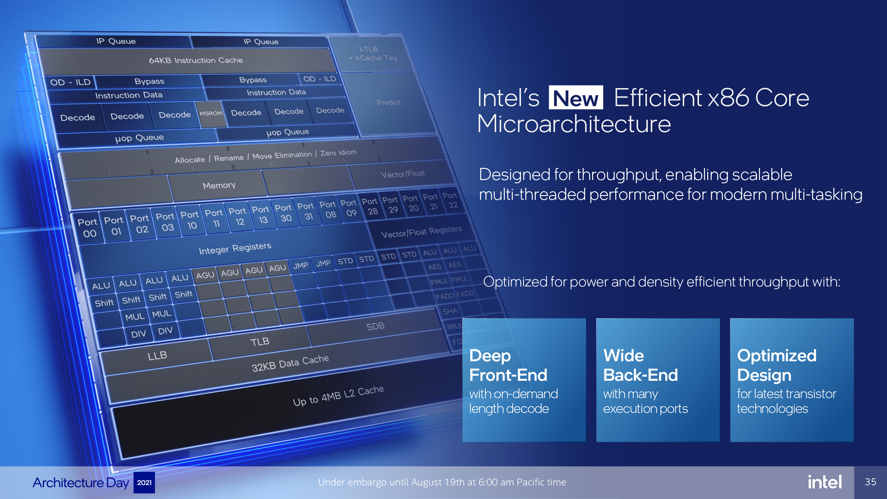
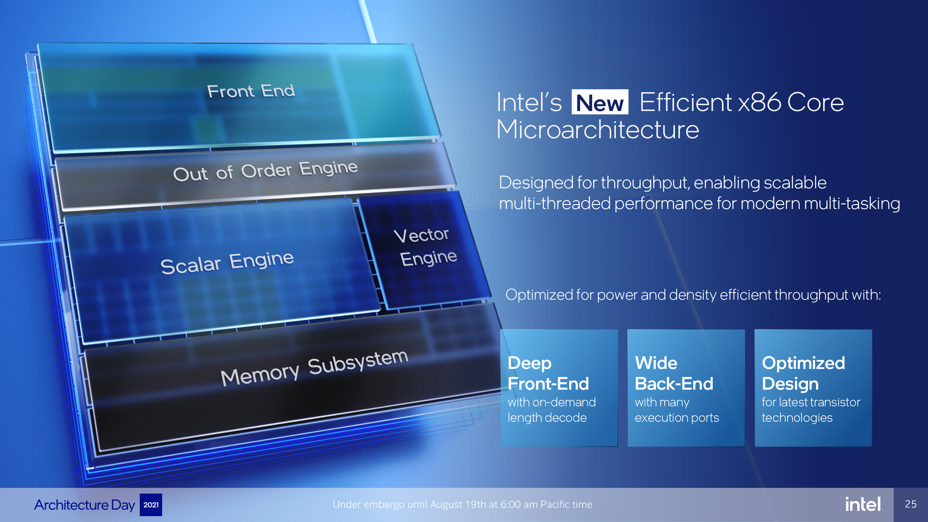
It all starts with a new way of thinking for x86 fries by pairing loftier-performance and high-efficiency cores within a single chip. That well-traveled design philosophy powers billions of Arm chips, frequently referred to as Big.Fiddling (Intel calls its implementation Big-Bigger), but it's a first for x86 desktop PCs. The Gilded Cove compages powers Alder Lake'southward 'big' loftier-operation cores, while the 'little' Atom efficiency cores come with the Gracemont architecture. Intel etches the cores on its 'Intel vii' process, marker the company's offset truly new node for the desktop since 14nm debuted six long years ago.
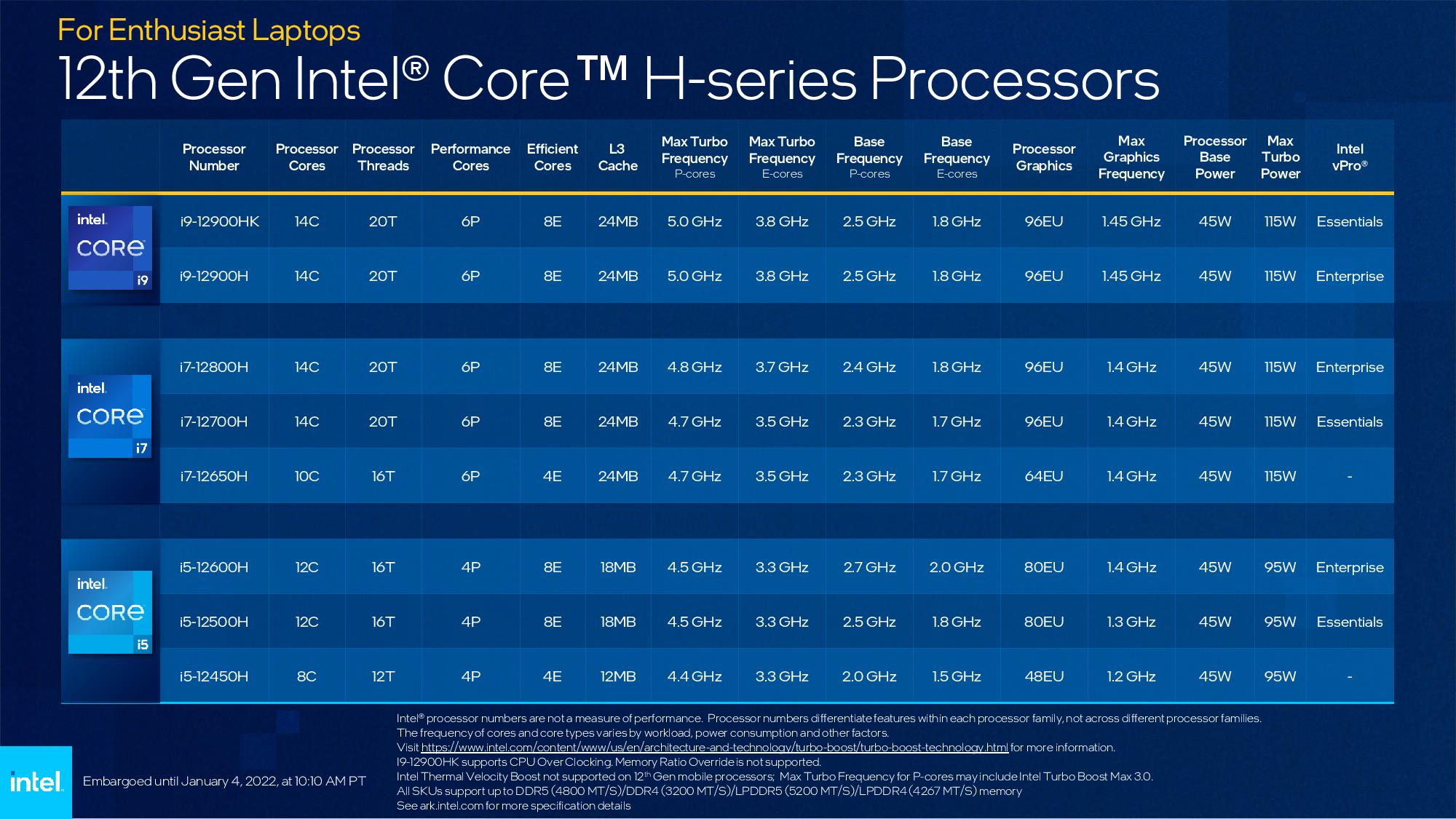
Intel is going all-in: the company will reunify its desktop and mobile lines with Alder Lake. Intel says it volition tune Alder Lake for high-performance, a must for desktop PCs and high-end notebooks. As evidenced past its opening salvo of 12th-Gen Alder Lake mobile lineup that tops out at xiv Cores and five.0 GHz, it appears the company has washed just that for mobile, too.
Potent adversaries claiming Intel on both sides. Apple'southward Arm-powered M1 processors take set a high bar for hybrid designs, outperforming all other processors in their class with the promise of more powerful designs to come. Meanwhile, AMD's Ryzen 5000 chips have taken the atomic number 82 over Intel's crumbling Skylake derivatives. Intel'due south Rocket Lake chips overtook AMD in unmarried-threaded operation, but they still trail in multi-core workloads due to Rocket Lake'south maximum of viii cores, while AMD has 16-core models for the mainstream desktop.
Intel certainly needs a come-from-behind design to thoroughly unseat its competitors, swinging the tables back in its favor like the Conroe fries did dorsum in 2006 when the Cadre architecture debuted with a ~forty% operation advantage that cemented Intel's potency for a decade. Intel's Raja Koduri has already likened the transition to Alder Lake with the debut of Core, suggesting that Alder Lake could indeed exist a Conroe-esque moment.
Intel'southward twelfth-Gen Alder Lake At a Glance
- Alder Lake is available now
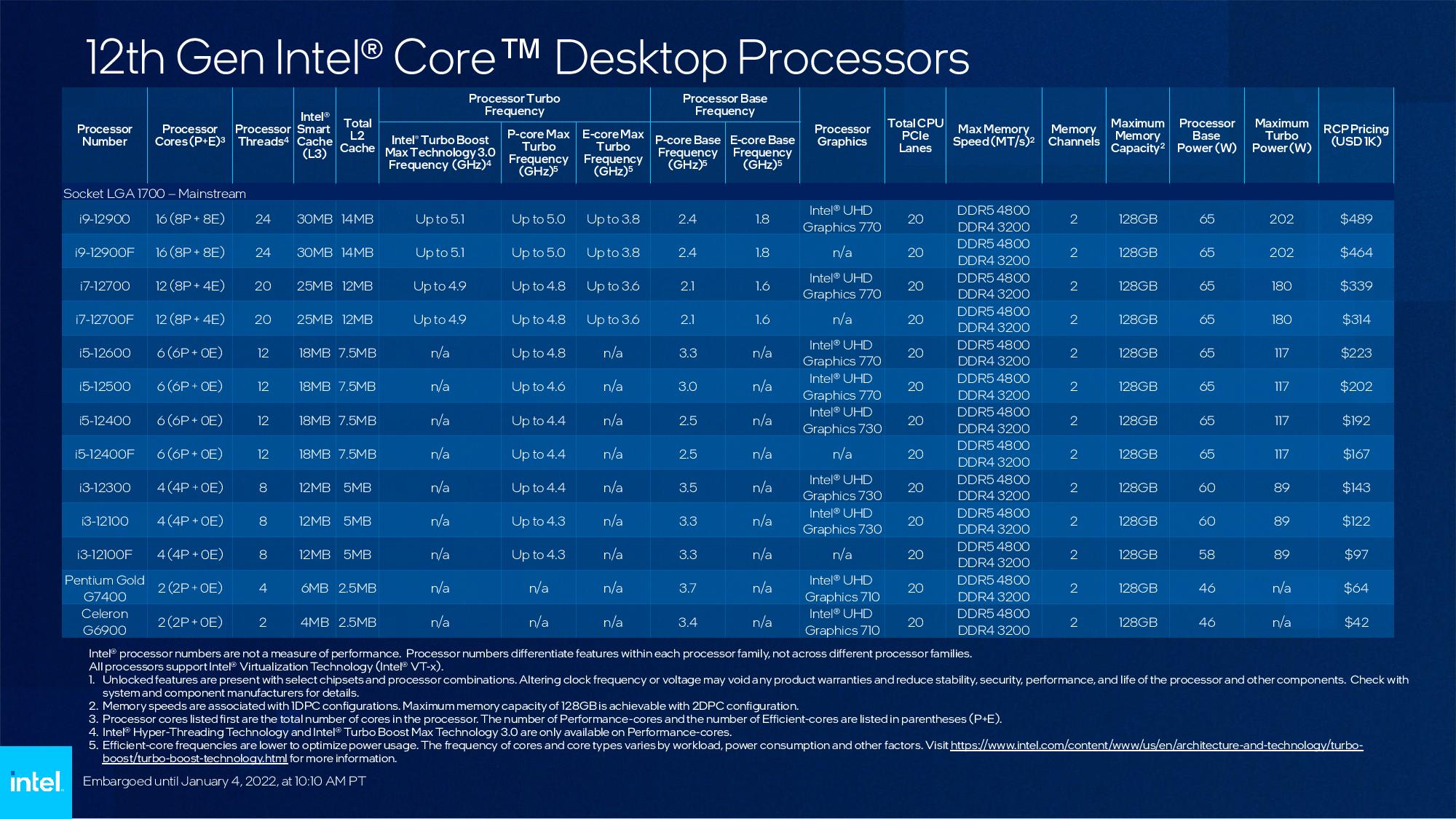
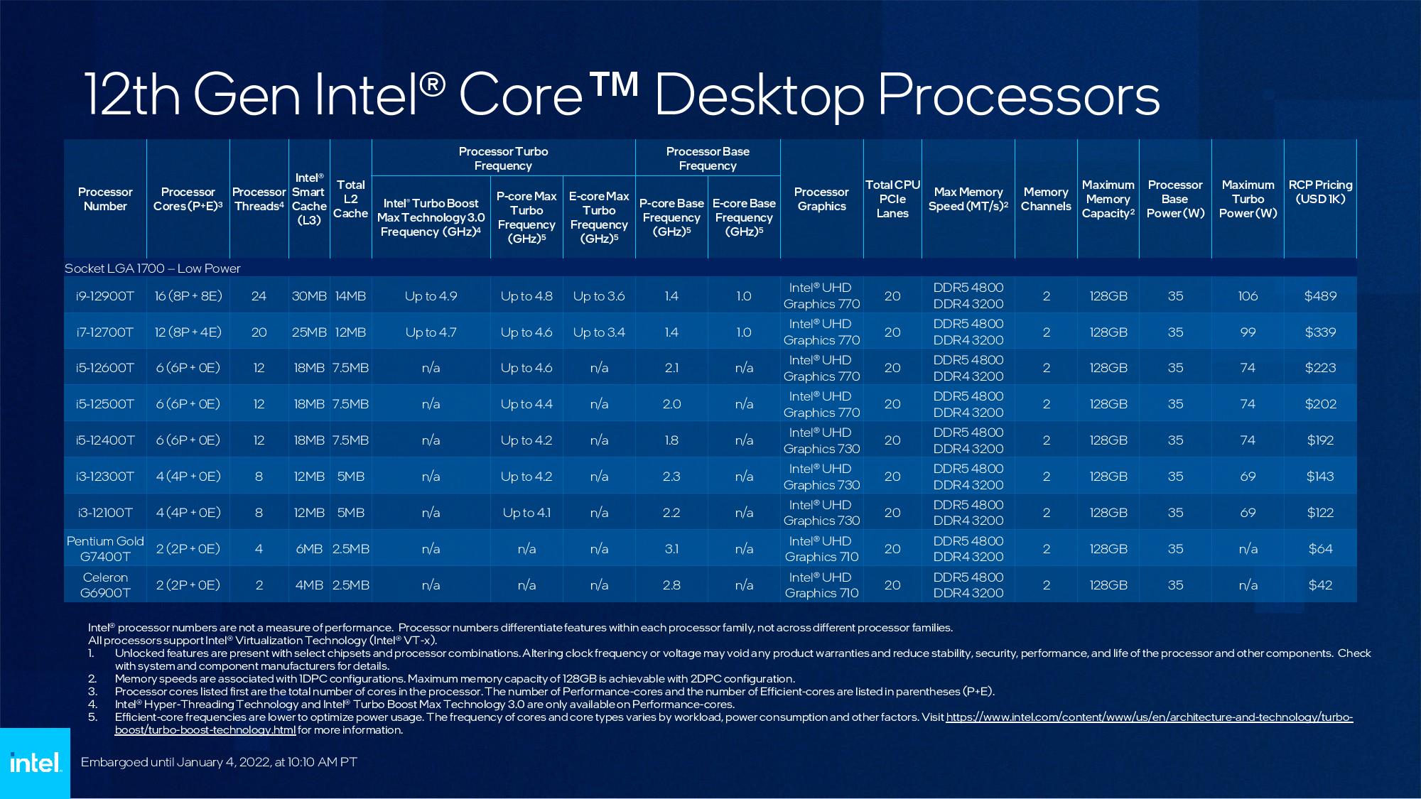
- Six flagship models: $589 Core i9-12900K, $409 i7-12700K, $289 i5-12600K. All 3 are also available as graphics-less KF models. Intel also has a range of 22 lower-priced models for desktop PCs.
- LGA1700 socket requires new motherboards
- The Alder Lake SoC will bridge from desktop PCs to ultramobile devices with TDP ratings from 9W to 125W, all built on the Intel vii process. The desktop PC comes with up to eight Performance (P) cores and eight Efficient (E) cores for a total of 16 cores and 24 threads and up to 30 MB of L3 cache for a unmarried chip.
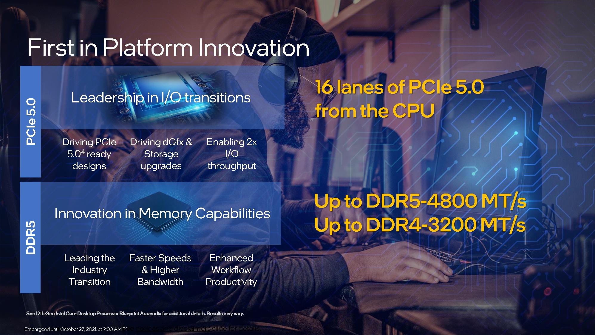
- Alder Lake supports either DDR4 or DDR5 (LP4x/LP5, too). Desktop PC supports x16 PCIe Gen 5 and x4 PCIe Gen four, while mobile supports x12 PCIe Gen 4 and x16 PCIe Gen three, Thunderbolt four, and Wi-Fi 6E.
- Intel'due south new hyper-threaded Performance (P) core, which comes with the Golden Cove microarchitecture designed for low-latency single-threaded performance, comes with an average of 19% more IPC than the Cypress Cove architecture in Rocket Lake. It also supports AVX-512 and AMX (a new AI-focused matrix-multiply ISA) for data center variants (both are disabled on consumer chips).
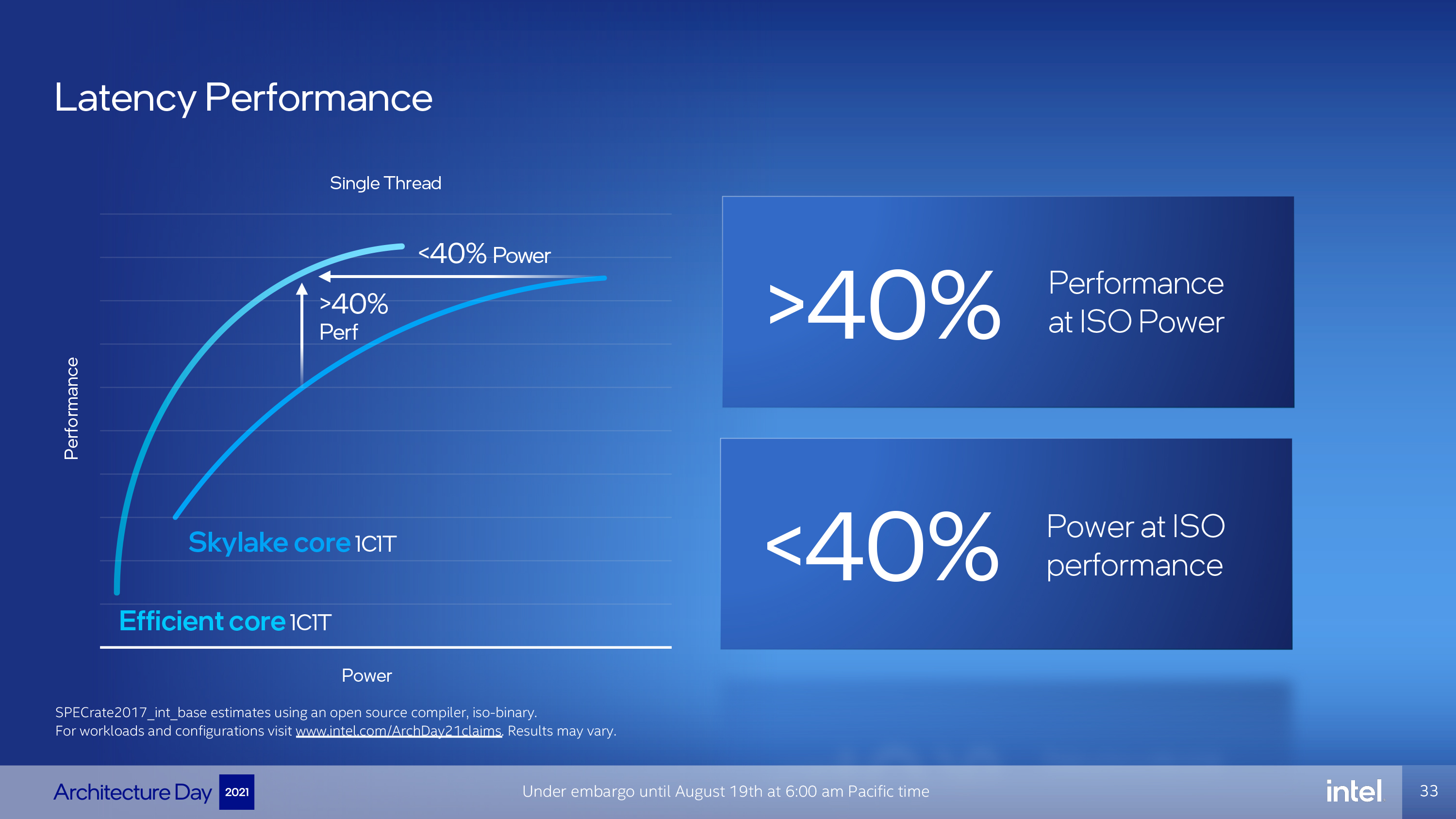
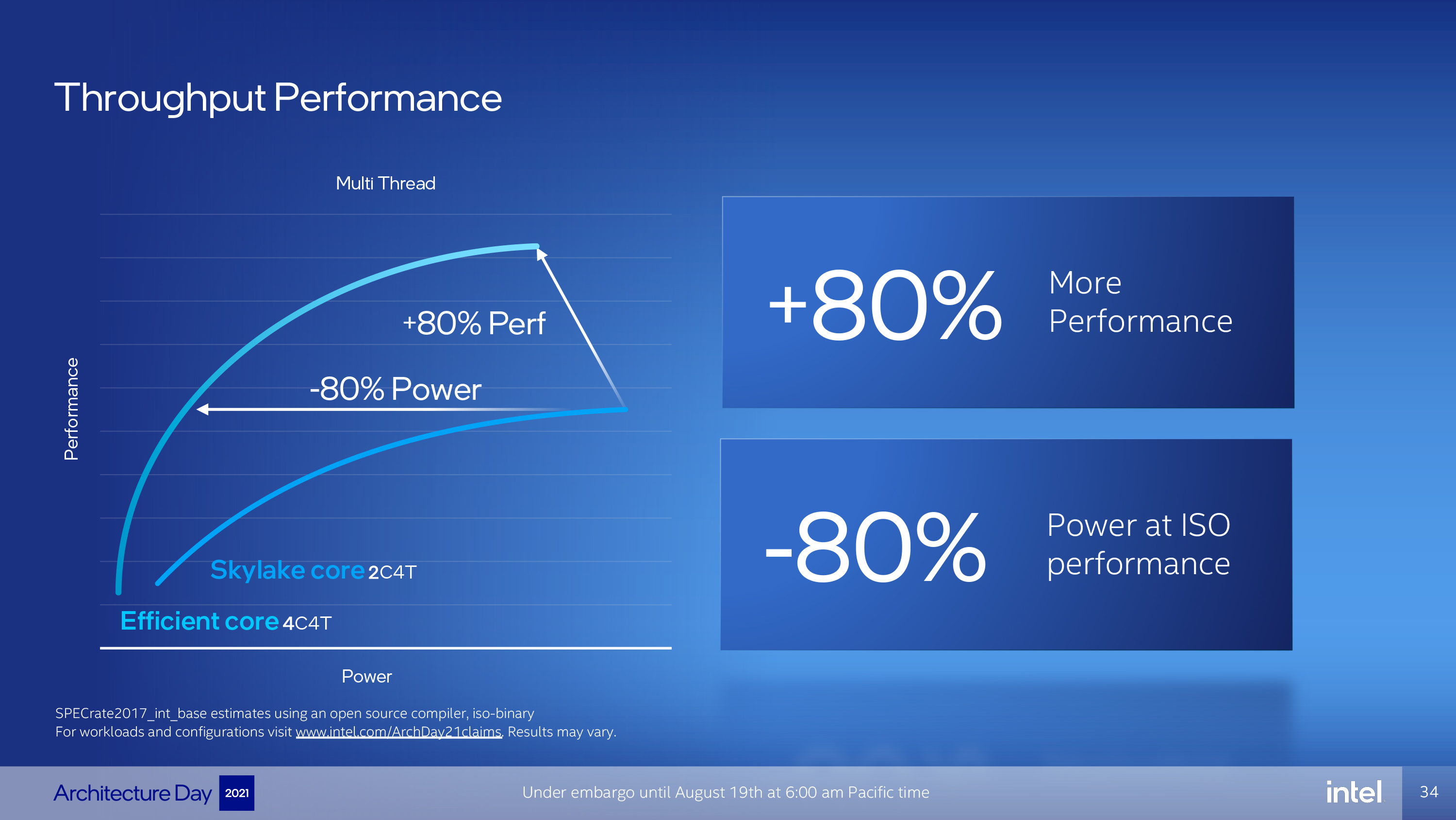
- Intel's new unmarried-threaded Efficiency (E) core comes with the Gracemont microarchitecture to improve multi-threaded functioning and provide infrequent area efficiency (small footprint) and performance-per-watt. 4 pocket-sized cores fit in the same area as a Skylake core and deliver lxxx% more performance in threaded work (at the same ability). A unmarried E core too delivers 40% more than operation than a single-threaded Skylake core (at the same power) in unmarried-threaded work (caveats apply to both).
- Intel's Thread Director is a hardware-based applied science that assures threads are assigned to either the P or Due east cores in an optimized manner. This is the sleeper tech that enables the hybrid architecture.
- 4 variants: -South for desktop PCs, -P for mobile, -K for low-ability devices, -Fifty Atom replacement, -N educational (probably Chromebooks)
Intel Alder Lake Release Date
The high-end Alder Lake One thousand-series processors for the desktop PC are now bachelor, just that only encompasses three SKUs and their graphics-less counterparts. Intel is expected to denote the full desktop PC stack, new chipsets for lower-end Alder Lake H670, B660 and H610 motherboards, and the laptop models at CES 2022.
Intel Alder Lake-S Desktop PC Specifications and Pricing
| U.S. Price | Cores | Threads | P-Core Base of operations/Boost | E-Core Base/Heave | TDP / PBP / MTP | DDR4-3200 | L3 Cache | |
| Ryzen 9 5950X | $799 | 16P | 32 threads | three.four / four.ix GHz | - | 105W | DDR4-3200 | 64MB (2x32) |
| Core i9-12900K / KF | $589 (K) - $564 (KF) | 8P + 8E | xvi Cores / 24 threads | iii.ii / 5.2 GHz | 2.4 / iii.nine GHz | 125W / 241W | DDR4-3200 / DDR5-4800 | 30MB |
| Ryzen 9 5900X | $549 | 12P | 24 threads | iii.7 / 4.viii GHz | - | 105W | DDR4-3200 | 32MB (1x32) |
| Cadre i9-11900K | $549 | 8P | 16 threads | 3.5 / v.3 GHz | - | 125W | DDR4-3200 | 16MB |
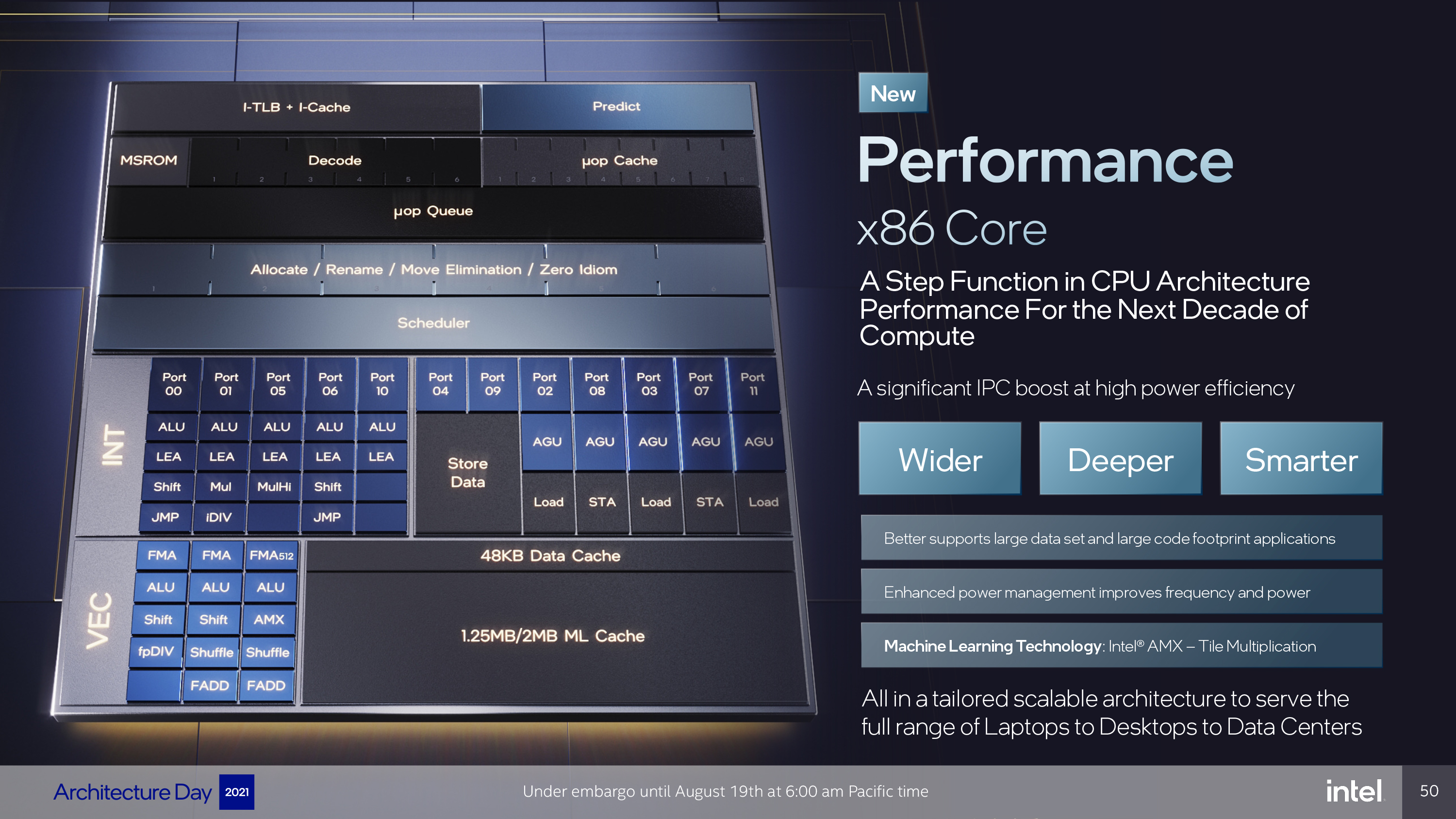
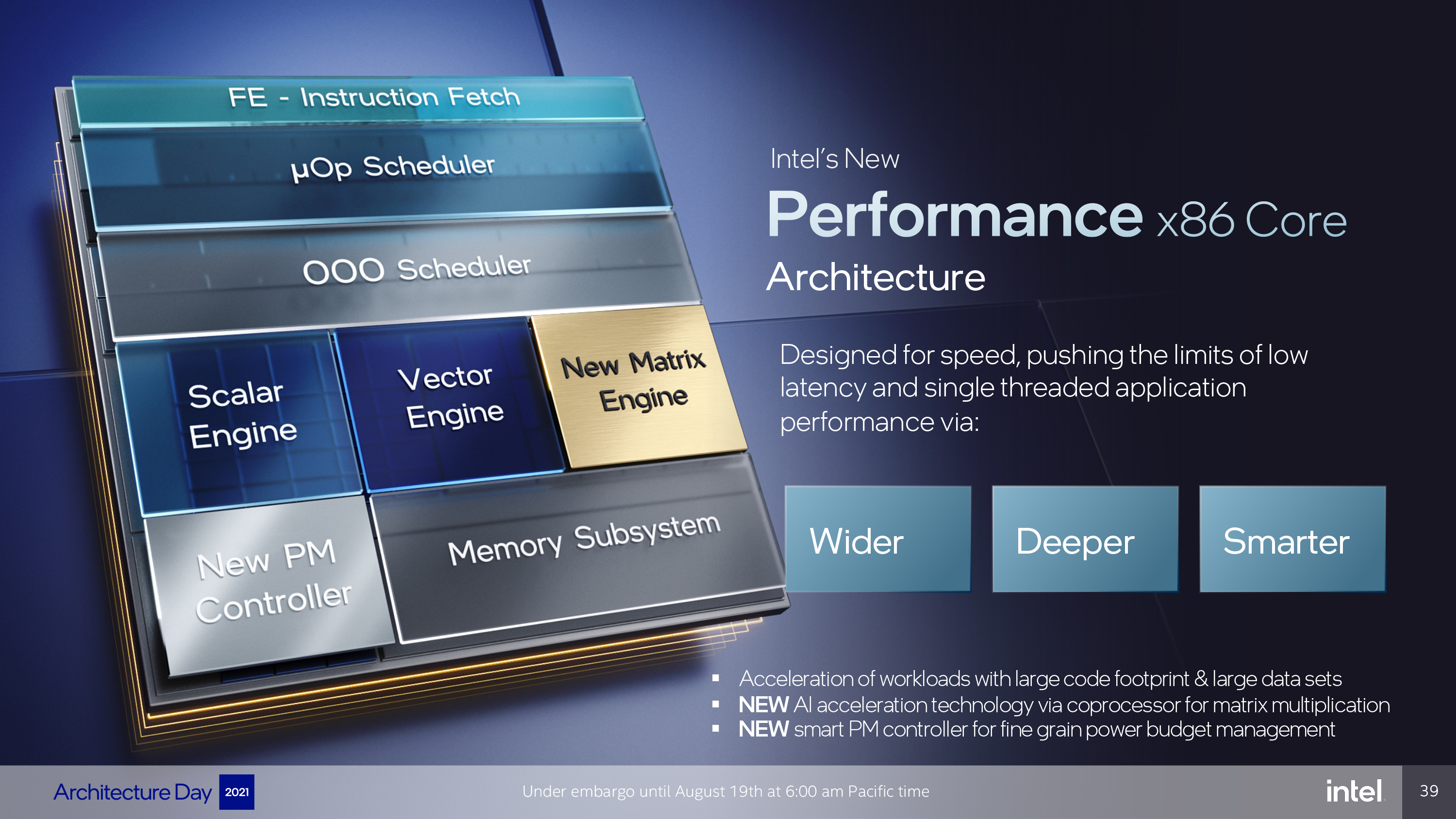
| Core i7-12700K / KF | $409 (M) - $384 (KF) | 8P + 4E | 12 Cores / 20 threads | 3.half-dozen / iv.9 GHz | ii.7 / 3.8 GHz | 125W / 190W | DDR4-3200 / DDR5-4800 | 25MB |
| Core i7-11700K | $409 | 8P | 16 threads | 3.six / v.0 GHz | - | 125W | DDR4-3200 | 16MB |
| Ryzen 7 5800X | $449 | 8P | 16 threads | 3.8 / 4.seven GHz | - | 105W | DDR4-3200 | 32MB |
| Core i5-12600K / KF | $289 (1000) - $264 (KF) | 6P + 4E | 20 Cores / 16 threads | 3.7 / four.9 GHz | 2.8 / iii.half dozen GHz | 125W / 150W | DDR4-3200 / DDR5-4800 | 16MB |
| Core i5-11600K | $272 | 6P | 12 threads | 3.ix / four.9 GHz | - | 95W | DDR4-3200 | 12MB |
| Ryzen 5 5600X | $299 | 6P | 12 threads | 3.7 / 4.6 GHz | - | 65W | DDR4-3200 | 32MB |
The Alder Lake fries use the Intel seven process, which used to be referred to as '10nm Enhanced SuperFin' before Intel recently renamed its process nodes during its latest procedure and packaging roadmap update. The Aureate Cove cores support Hyper-Threading, allowing ii threads to run on a single core, while the smaller Gracemont cores are single-threaded. That means some models could come with seemingly-odd distributions of cores and threads. All Alder Lake chips support DDR4-3200 or DDR5-4800.
Intel's $589 16-cadre Cadre i9-12900K comes with eight P-cores that support hyper-threading, and eight single-threaded E-cores for a total of 24 threads. That's a 33% increase in thread count over the previous-gen Cadre i9-11900K. The P-cores accept a three.2 GHz base, and meridian frequencies reach 5.ii GHz with Turbo Heave Max 3.0 (this feature is simply on P-cores). This scrap comes with 125W PBP (base) and 241W MTP (peak) power ratings.
The 12900K has a 100 MHz reduction in peak clock frequency compared to the 11900K, just that isn't too meaningful given the entirely new hybrid architecture — these chips volition realize performance gains from using different core types for different tasks. Speaking of which, the E-cores have a two.4 GHz base and stretch up to three.ix GHz via the standard Turbo Boost two.0 algorithms. The chip comes armed with 30MB of L3 cache and 14MB of L2.
At $589, the Core i9-12900K comes at a $forty premium over its prior-gen analogue, squeezing in between the $799 16-core Ryzen 9 5950X and $549 Ryzen 9 5900X. That could be bonny if Intel's performance claims pan out (more later), but it leaves a sizeable $185 gap between the Core i9 and i7 families that Intel inadequately plugs with the graphics-less $564 Core i9-12900KF. It's logical to expect a filler product between Cadre i7 and i9 in the futurity (possibly like the Core i9-10850K).
The $409 Core i7-12700K comes with the same $409 tray pricing as the previous-gen Core i7-11700K and has eight P-cores and iv Eastward-cores, for a full of xx threads. The P-cores run at a 3.half dozen / 5.0 GHz base/boost, while the E-cores weigh in at two.vii / 3.8 GHz, all fed by 25MB of L3 enshroud and 12MB of L2. The graphics-less $384 Core i7-12700KF comes with a $25 price reduction.
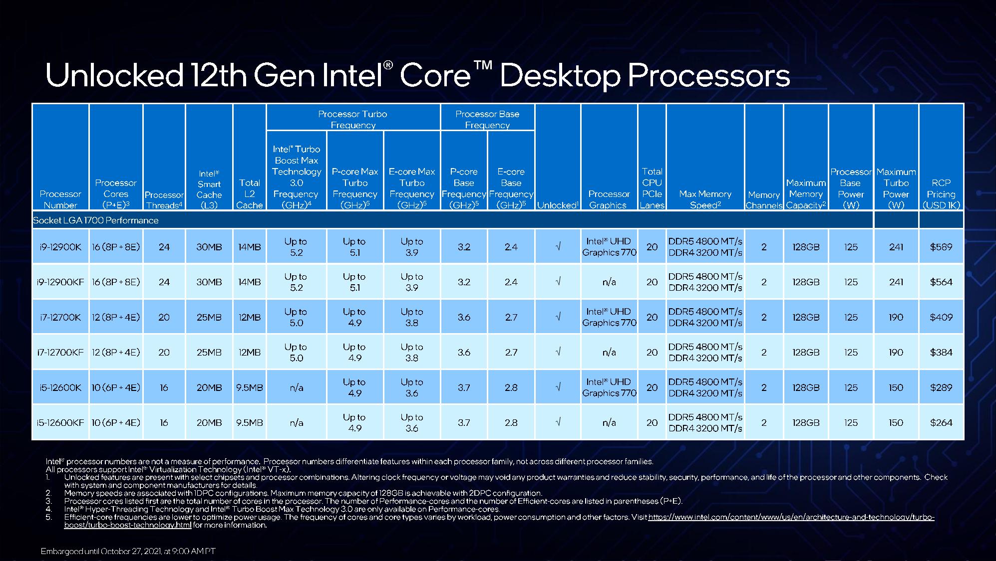
The 12700K's $409 price point means that Intel has kept the Core i7 flagship at its same price point, where it lands between the $449 Ryzen vii 5800X and $399 Ryzen five 5600X. The 12700K/F's increased operation could make it a more attractive office than its lackluster previous-gen counterpart, the hard-to-recommend Core i7-11700K.
The Core i5-12600K's $289 price point remains the same as the prior-gen Core i5-11600K, meaning it lands correct smack dab in gamer country, going toe-to-toe with the $299 six-core Ryzen 5 5600X and representing the lowest point of entry to the Alder Lake family unit (at least for now). This flake comes with half-dozen threaded P-cores that operate at 3.7 / 4.ix GHz and four Eastward-cores that run at ii.8 / 3.six GHz, for a total of 16 threads. That's paired with 20MB of L3 and 9.5MB of L2 cache.
AMD's competing Ryzen v 5600X currently leads our Best CPU for gaming list, but it faces a stiff claiming from Intel's 12600K.
All the Alder Lake chips support both DDR4 and DDR5 retentivity, only there are several caveats to the listed DDR5 support. As a default, DDR5 runs in Gear 2 mode, resulting in college latency, and standard motherboards but back up DDR5-4800 if the motherboard has merely two physical slots. Therefore, at stock settings, the chip will only support DDR5-4400 on whatever motherboard with 4 slots, even if only two slots are populated.
Intel has discarded its 'TDP' (Thermal Design Point) nomenclature, and now assigns a Processor Base Power (PBP) metric in its identify. The company besides added a secondary Maximum Turbo Power (MTP) metric to its spec sheets to quantify the highest power level during boost action (typically chosen PL2).
Alder Lake'due south new retention controllers support four unlike memory types: DDR5-4800 and LP5-5200, along with DDR4-3200 and LP4x-4266. This single design's broad memory back up enables different types of retentivity configurations for unlike utilise-cases. It appears that Intel will split its retentivity support into DDR4 for lower-end Z690 motherboards, B- and H-series models, and mobile systems, while DDR5 volition only slot in for the highest-end Z-series motherboards. This makes sense given the expected loftier pricing for DDR5 retentivity in the early days of adoption, though it'southward notable that Intel hasn't confirmed its arroyo all the same.
Alder Lake also supports up to PCIe 5.0 with 64 GB/s of throughput across a x16 lane connexion. The desktop PC fries support a x16 PCIe Gen 5 connection with an boosted x4 PCIe Gen 4 connection (it is unclear if this x4 connection is used for the chipset or exposed to the user), while lower-power models support a x12 PCIe Gen four config paired with a x16 PCIe Gen 3 connexion.

The first fries based on the design come in three different packages, each for a different segment: The desktop PC flake that will drop into new motherboards with an LGA 1700 CPU socket (yes, 115x coolers with converters are compatible), a high-performance BGA Type3 bundle for mobile applications (this is probable a 12-28W UP3 package, though Intel hasn't confirmed), and a high-density BGA Type4 HDI package for Ultra Mobile applications (likely a 7-15W UP4 equivalent for ultra-thins).
We take also learned that the Intel Alder Lake fries for desktop PCs volition come with two die variants, with one being a six-core with p-cores only, while the other will come up with the standard (up to) eight p-cores and viii east-cores.
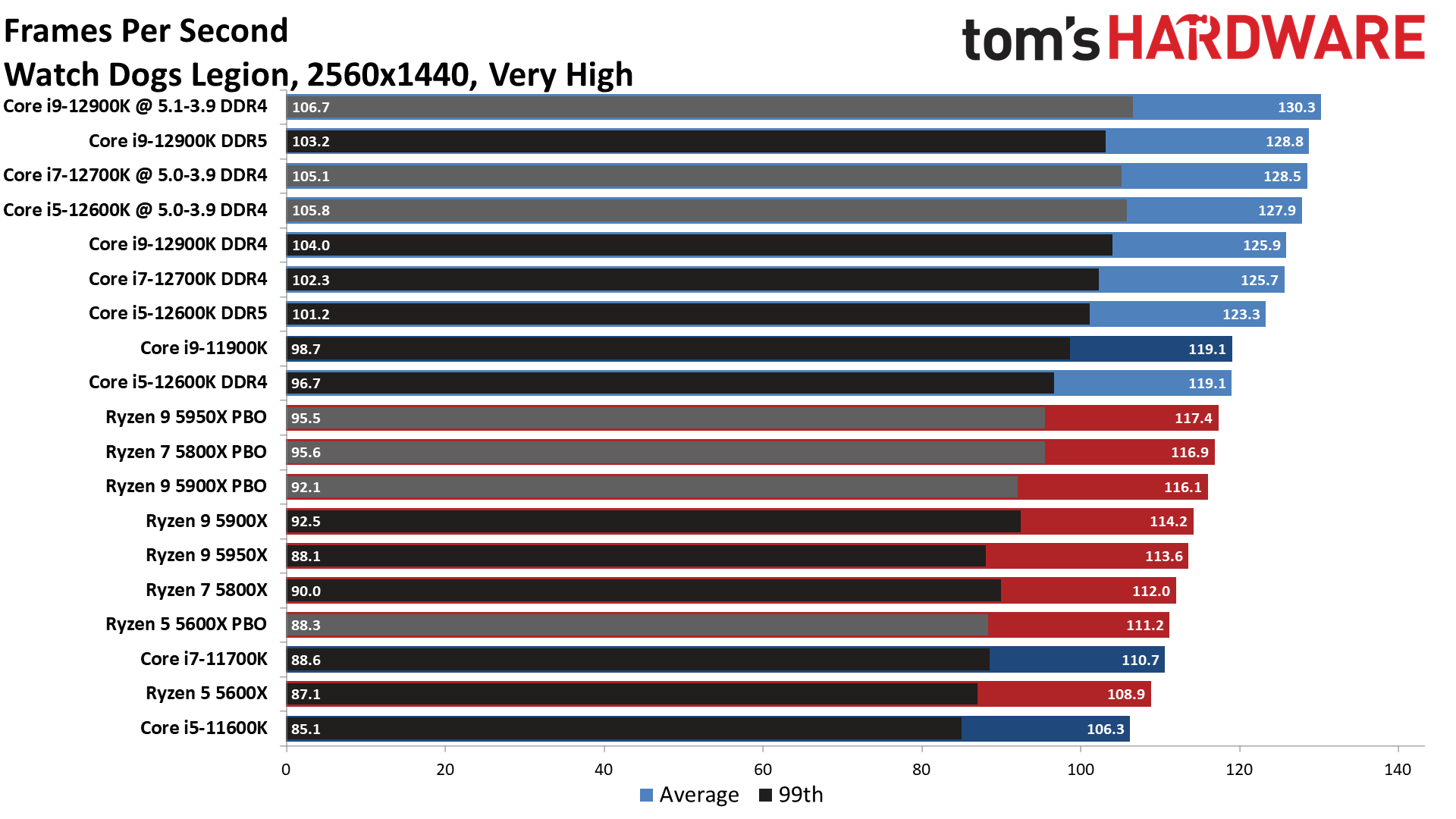
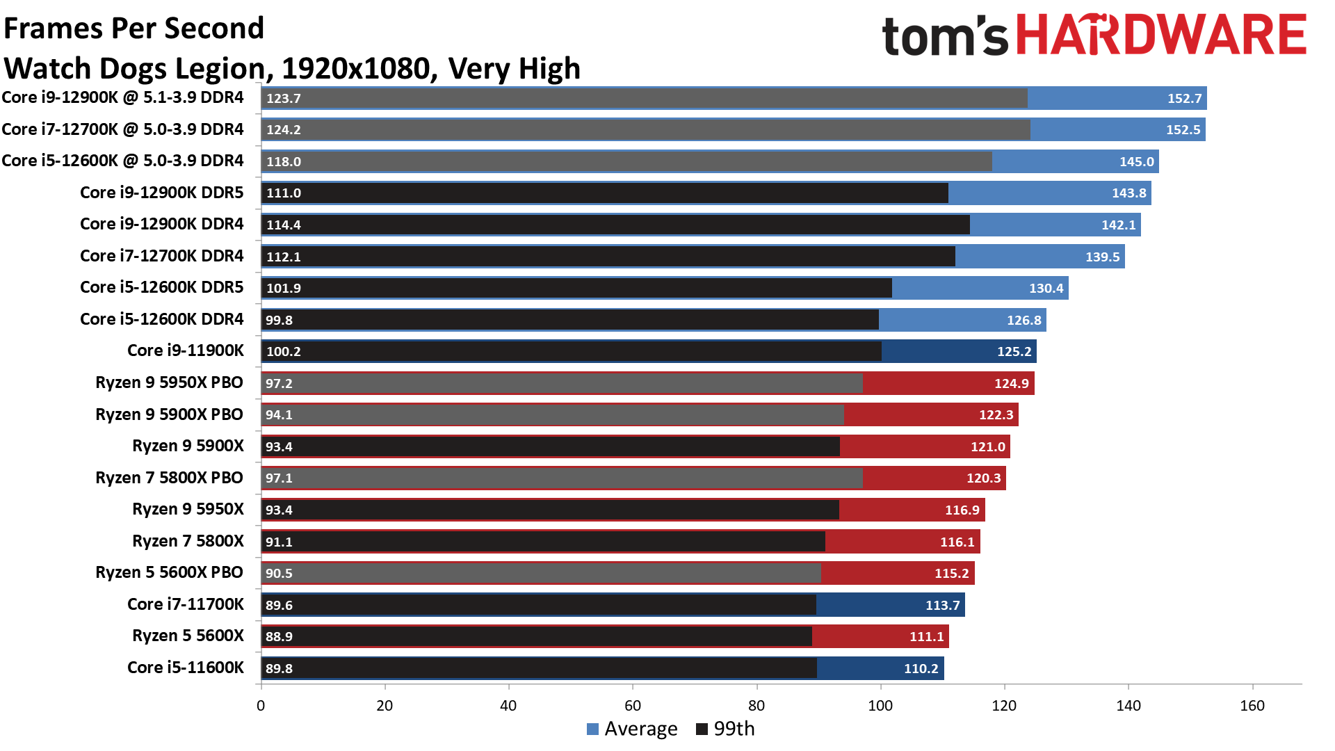
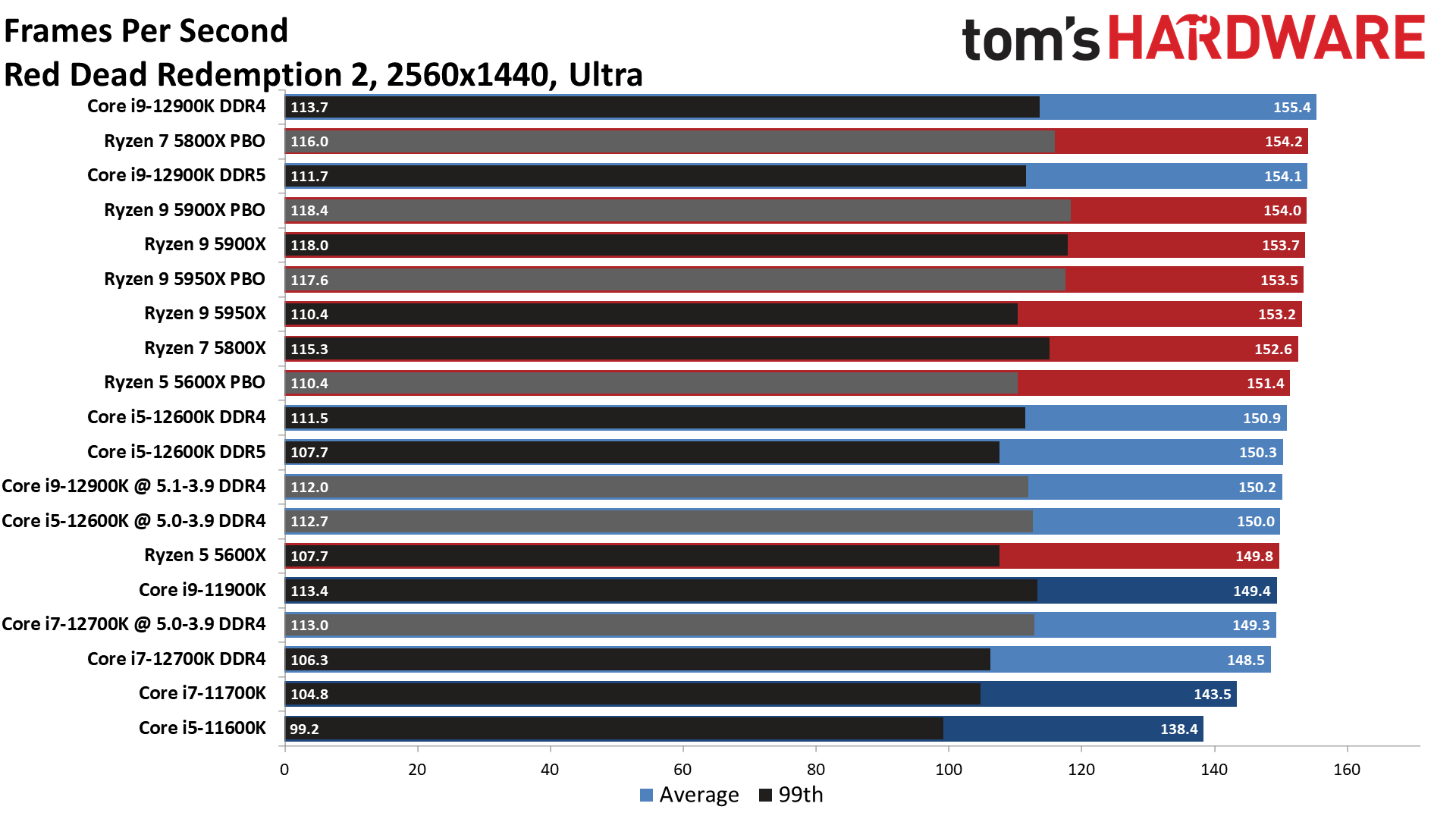
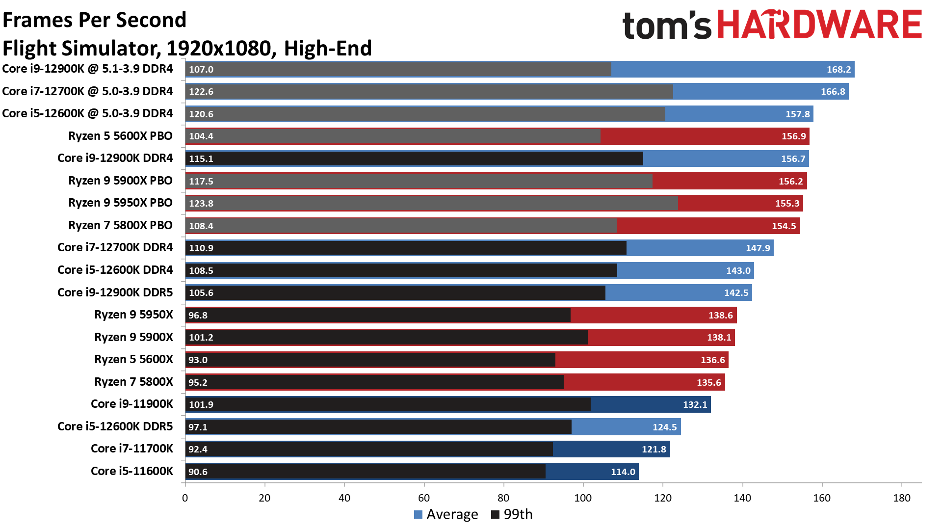
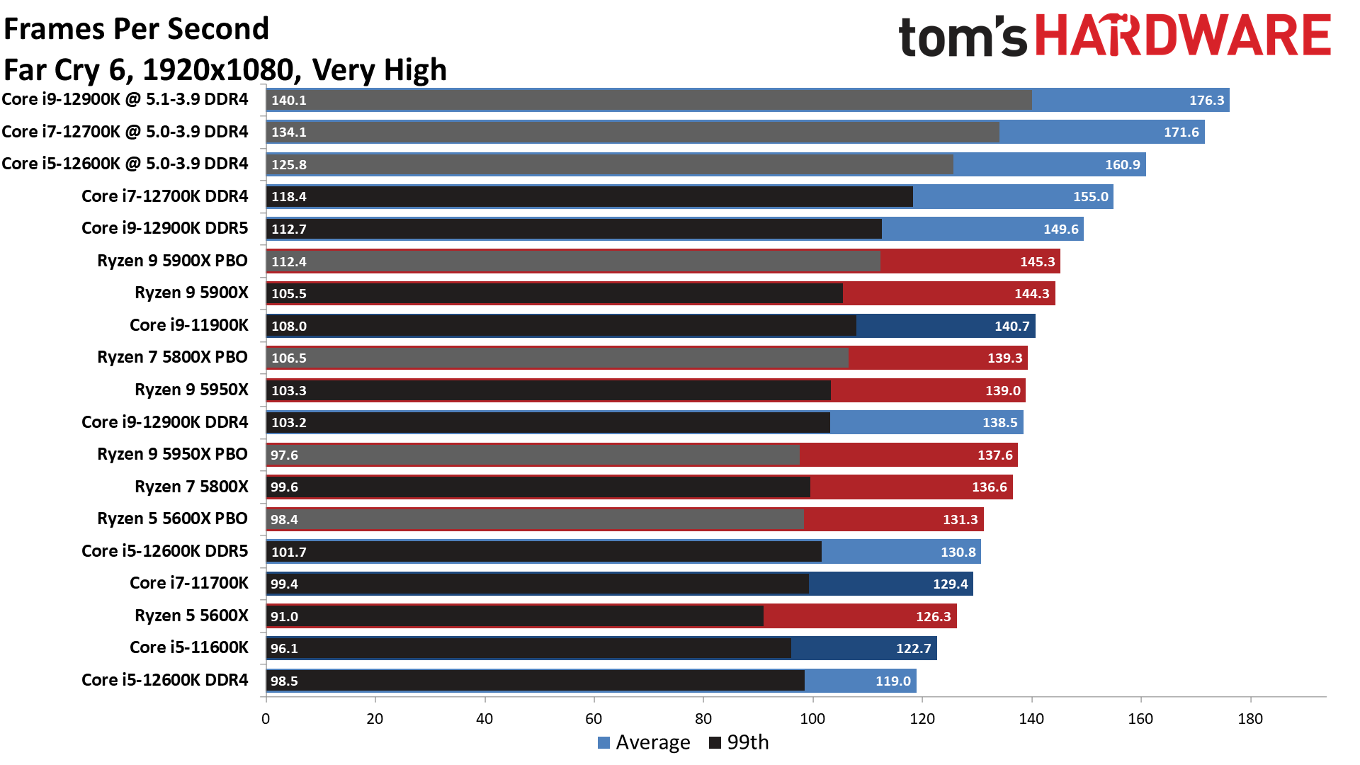
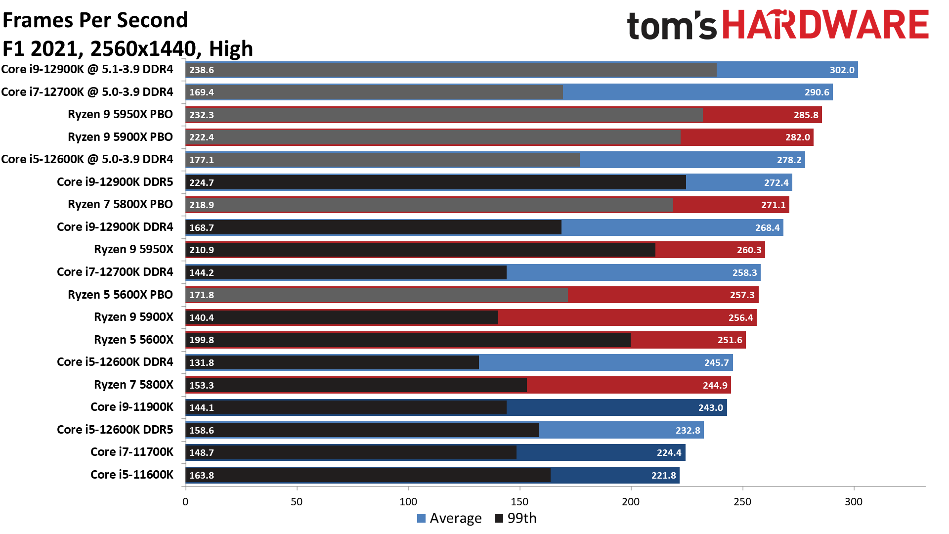
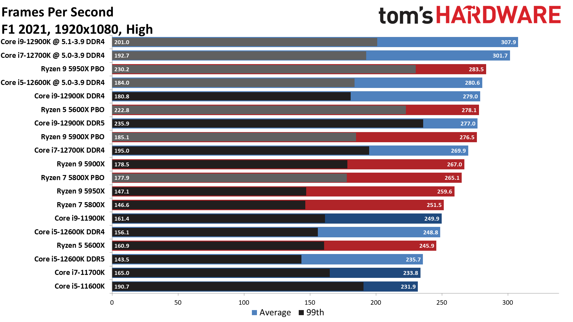
Intel Alder Lake Gaming Benchmarks and Performance
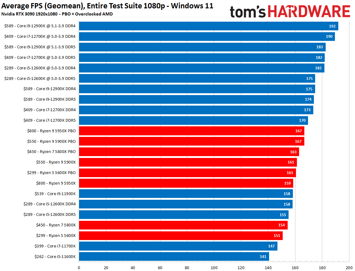
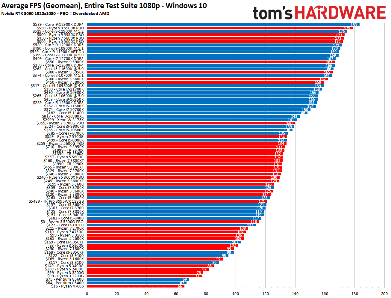
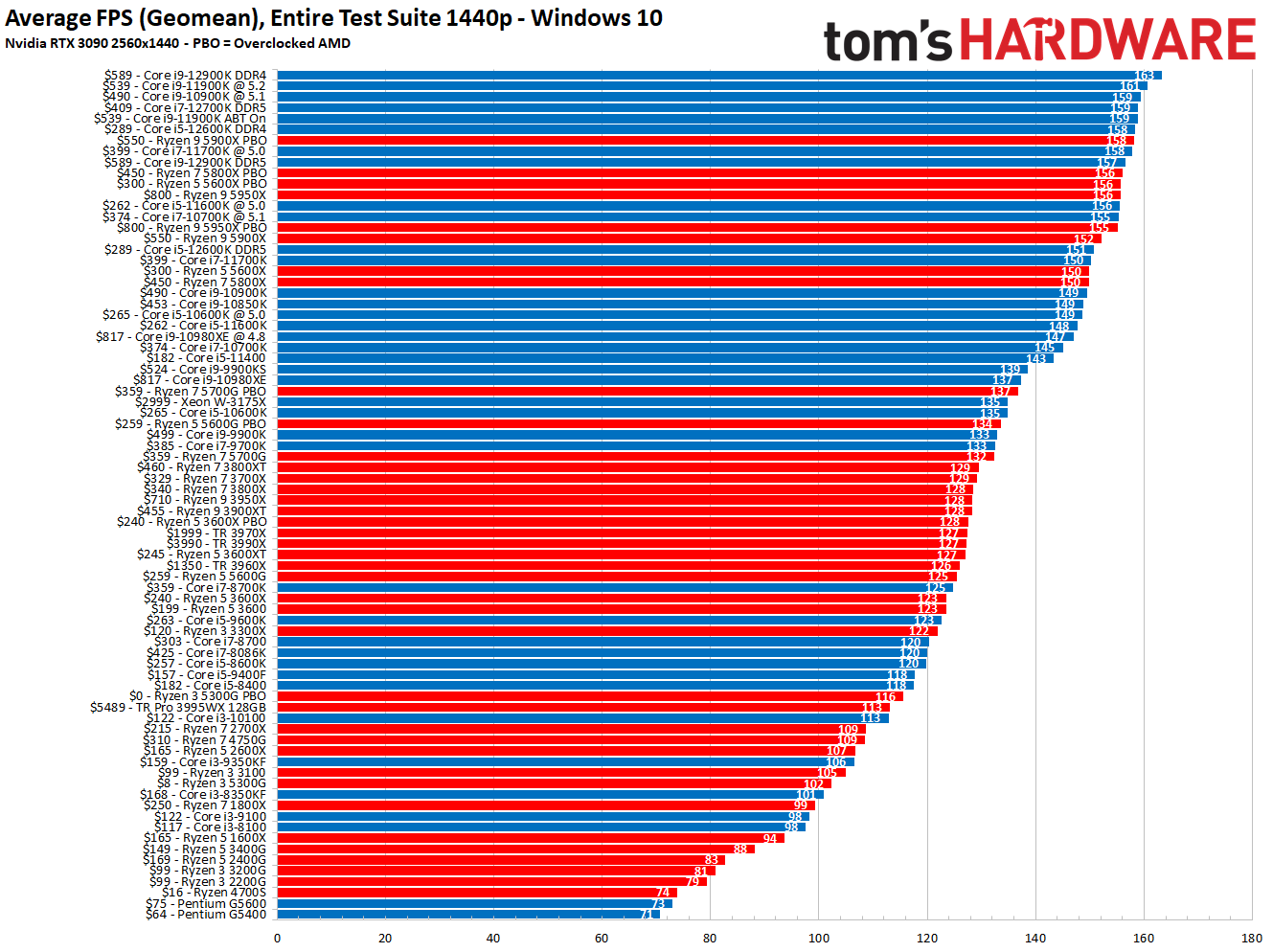
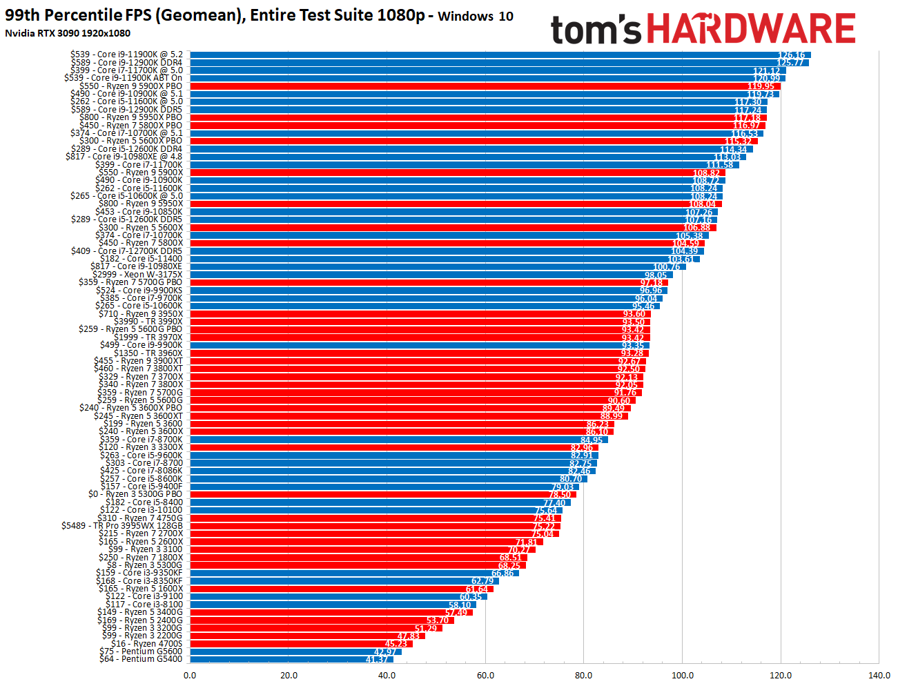
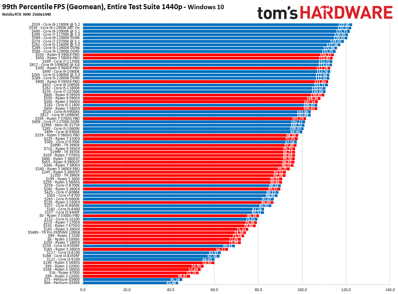
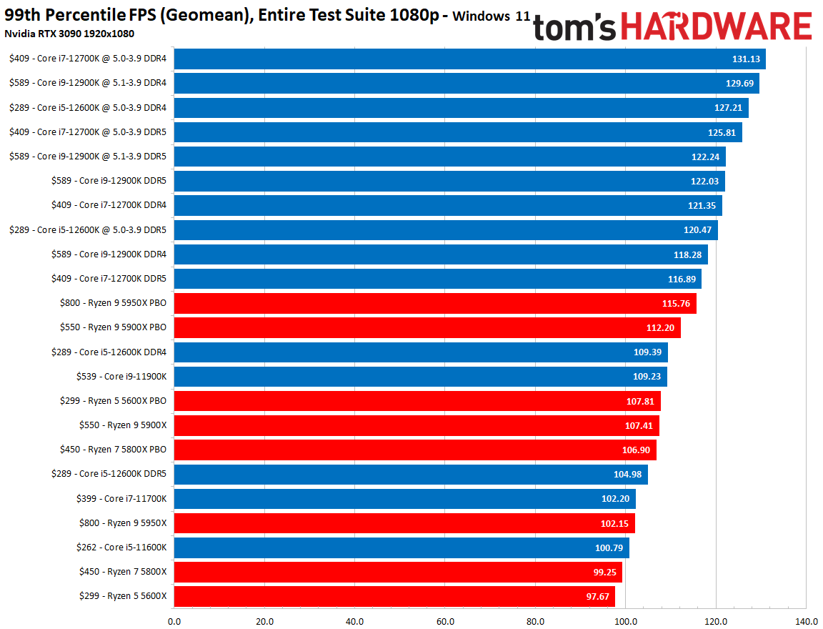
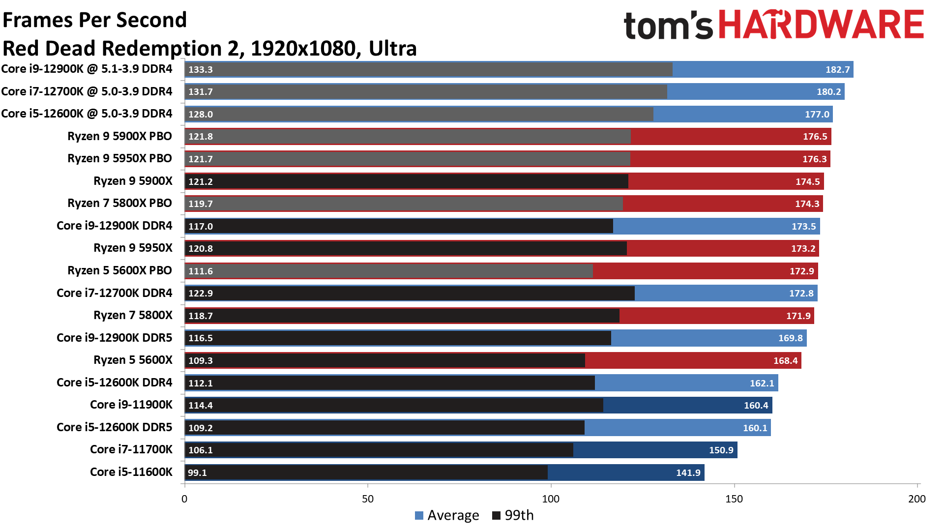
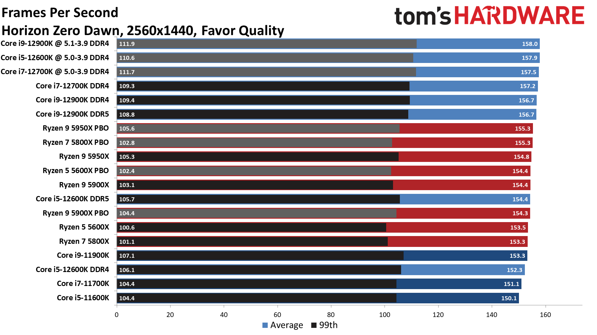
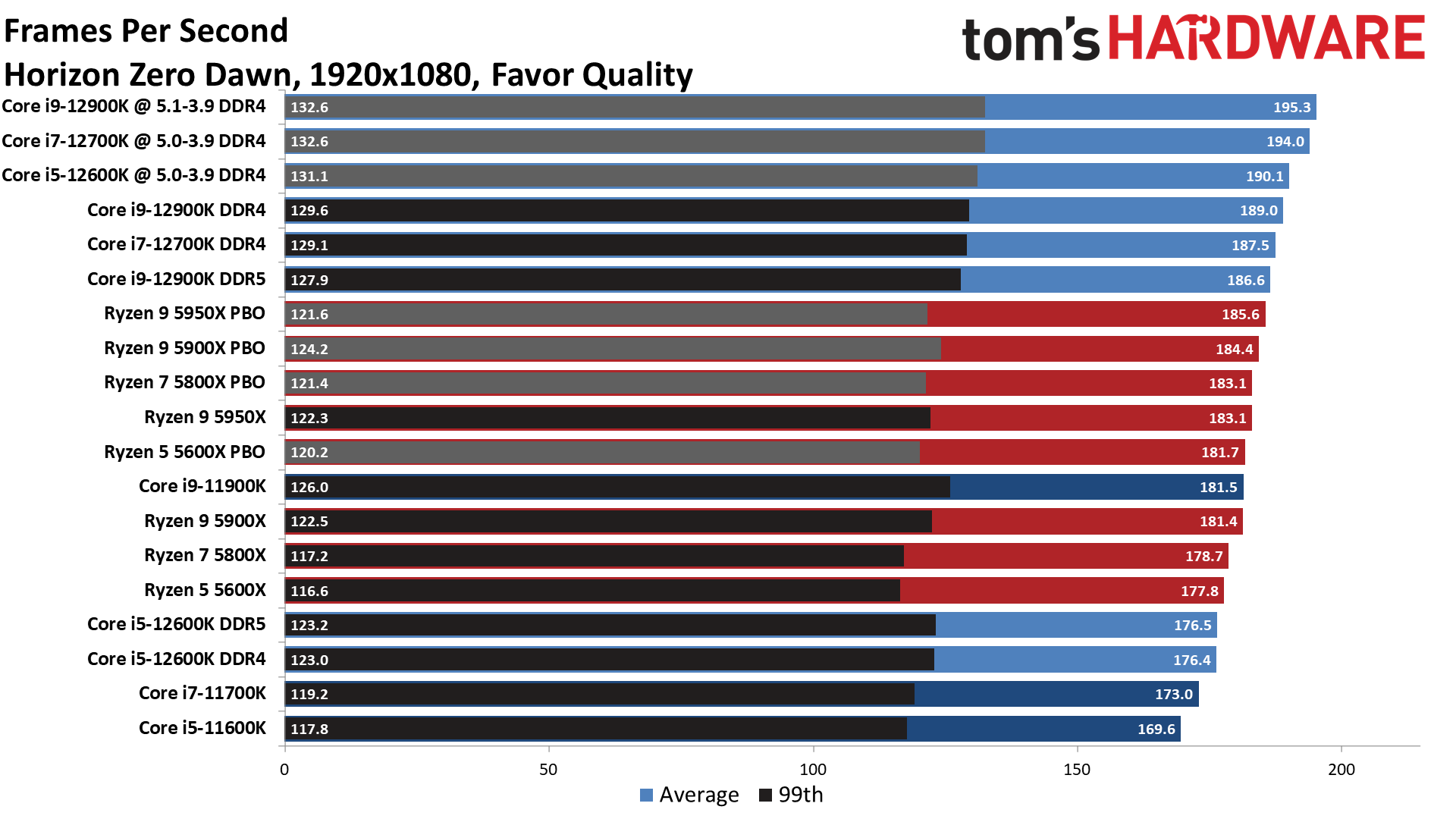
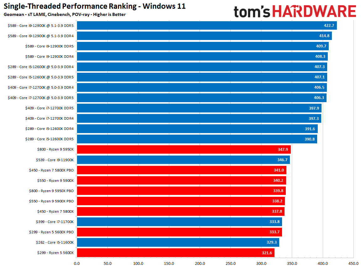
Here's the overall testing from our review, which has additional analysis. Above you tin see gaming results in both Windows 11 and Windows 10. The $549 12-core Ryzen 9 5900X is AMD's fastest gaming chip, but the $589 Cadre i9-12900K is 8.7% faster in the cumulative 1080p gaming measurement across our entire exam suite. And that's with both the DDR4 and DDR5 retention configurations, so you won't have to drop serious cash on a DDR5 kit to go at that place.
Stepping down $300, the $289 Core i5-12600K with DDR5 memory is ~ii.7% faster than the $299 Ryzen v 5600X, merely that gap widens slightly with less expensive DDR4 memory. The Core i5-12600K also finer ties the Ryzen seven 5800X, but for $161 less.
Rocket Lake buyers will exist plenty disappointed. The Core i9-11900K landed a mere six months agone at $539, but the 12900K is ~11% faster in gaming. It's also much faster in the threaded workloads that we'll encounter later in our application testing. Nosotros see a similar story unfold with the Cadre i5-11600K compared to the 12600K, with nine% more performance in gaming coming for $27 more.
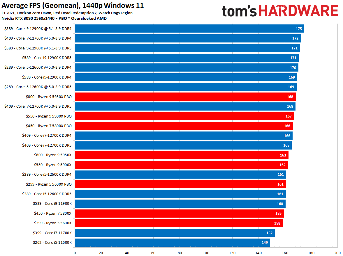
Naturally, moving over to 1440p brings a GPU clogging into the equation, so the performance deltas between the fries shrink tremendously. Here the Core i5-12600K finer ties the 5600X and 5800X, while the 12900K is a mere 3.half-dozen% faster than the Ryzen 9 5950X.
The Core i9-12900K slots in as the fastest gaming bit on the planet, toll exist damned, but the Core i7-12700K delivers basically the same gaming functioning for far less cash, making it the go-to selection for functioning addicts. For mainstream gamers, the Core i5-12600K offers the best blend of price and functioning that yous can find on the market, bar none.
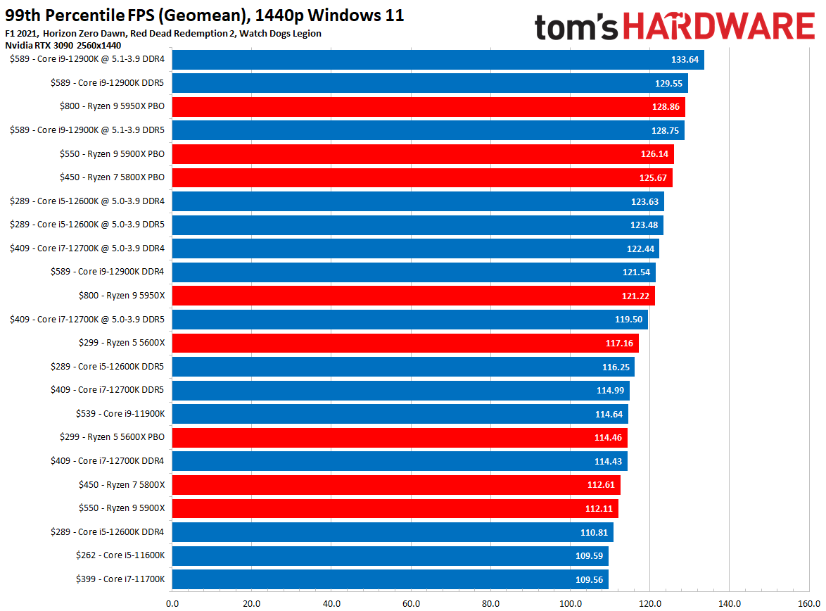
Flipping through the 99th percentile charts shows larger deltas, but we have to view those with caution as Windows xi is still young and seems to suffer from more framerate variability than our Windows ten test platform. This could event from yethoped-for-updated game code, the relatively new graphics drivers for Windows xi, or some other combination of factors that could exist smoothed out in the time to come.
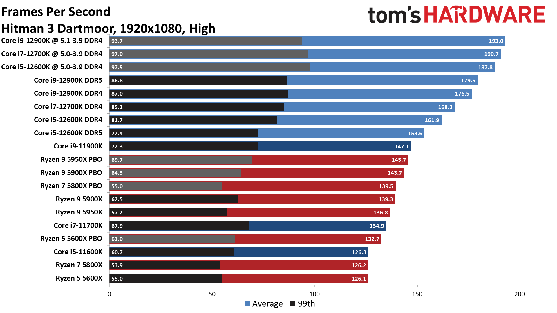
Intel's Alder Lake carves out a win in Windows 11, just large performance deltas in a few of the game titles tin heavily impact these types of cumulative measurements. For instance, Intel enjoys a sizeable pb in Hitman three, but that game is specifically tuned to leverage the Due east-cores effectively past offloading low-priority tasks similar physics to the small-scale cores. That can be seen as an advantage by some because more game devs could take this arroyo, or every bit a fluke by others that think this type of optimization will simply come to Intel-sponsored titles.
The competition between Intel and AMD is absolutely closer now, so it's best to make an informed decision based on the types of titles you play ofttimes. Be sure to check out the private tests below.
Intel Alder Lake Application Benchmarks
We can boil down productivity application functioning into two broad categories: unmarried- and multi-threaded. These slides show the geometric hateful (equal weighting to all tests) of functioning in several of our well-nigh important tests in each category, but be sure to look at the expanded results below.
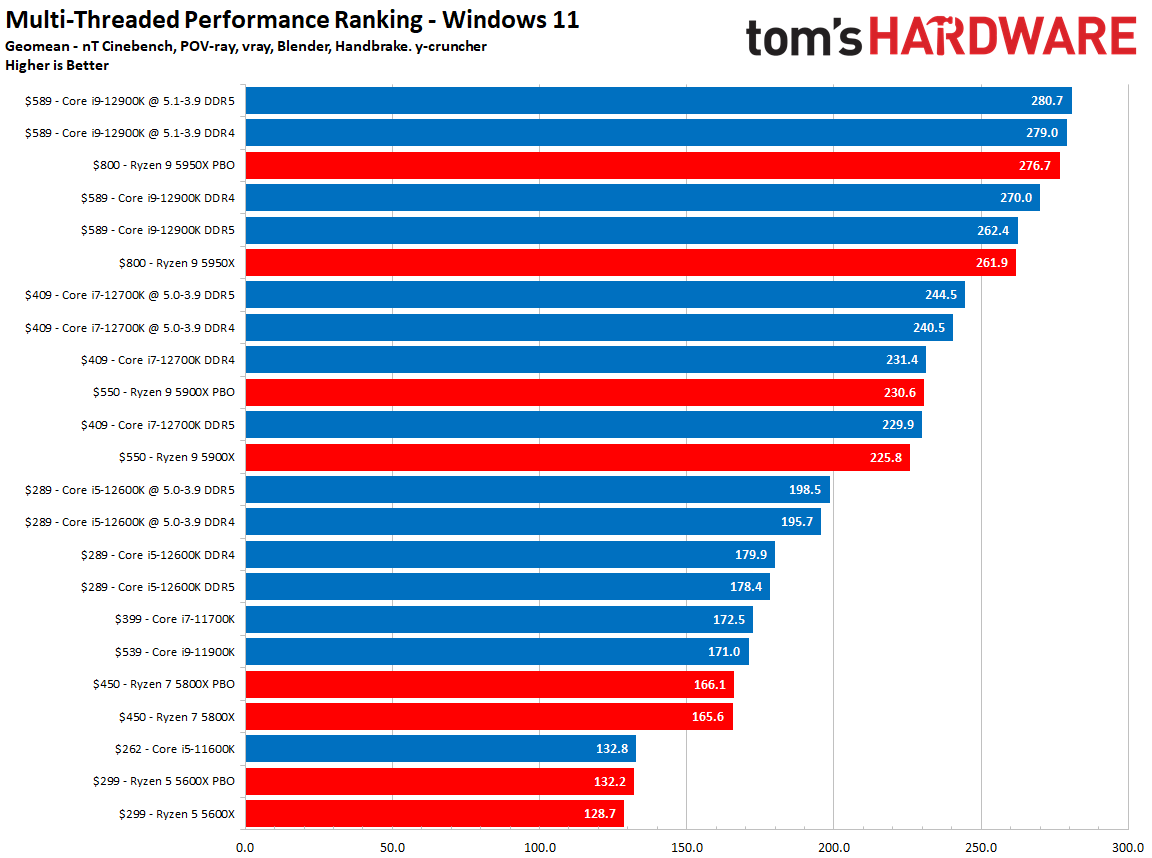
Alder Lake delivers a few stunning wins in the threaded workloads that Ryzen has dominated for so long, highlighting the advantages of the x86 hybrid compages. It is quite surprising to encounter the 24-thread Core i9-12900K with DDR5 retention necktie the 32-thread Ryzen nine 5950X in the multi-threaded ranking, but even more than surprising to meet information technology take a iii% lead with DDR4. That's pretty impressive in light of the 5950X'due south $800 price tag.
The Cadre i5-12600K is every bit impressive in its price range as it is 38% faster in threaded work than the comparably-priced 5600X, and 7% faster than the 5800X that costs $161 more.
The deltas in favor of Alder Lake are fifty-fifty more than convincing in the unmarried-threaded metric, but y'all shouldn't put undue importance on this metric because it is comprised of a few very specific workloads. Y'all can see a broader spate of lightly-threaded workloads beneath. Needless to say, Alder Lake dominates those types of workloads. Bank check out our review for the blow-by-blow on all of the different benchmarks.
Intel Alder Lake Ability Consumption, Efficiency, and Thermals
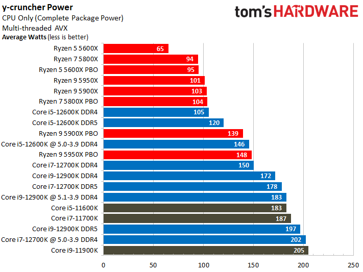

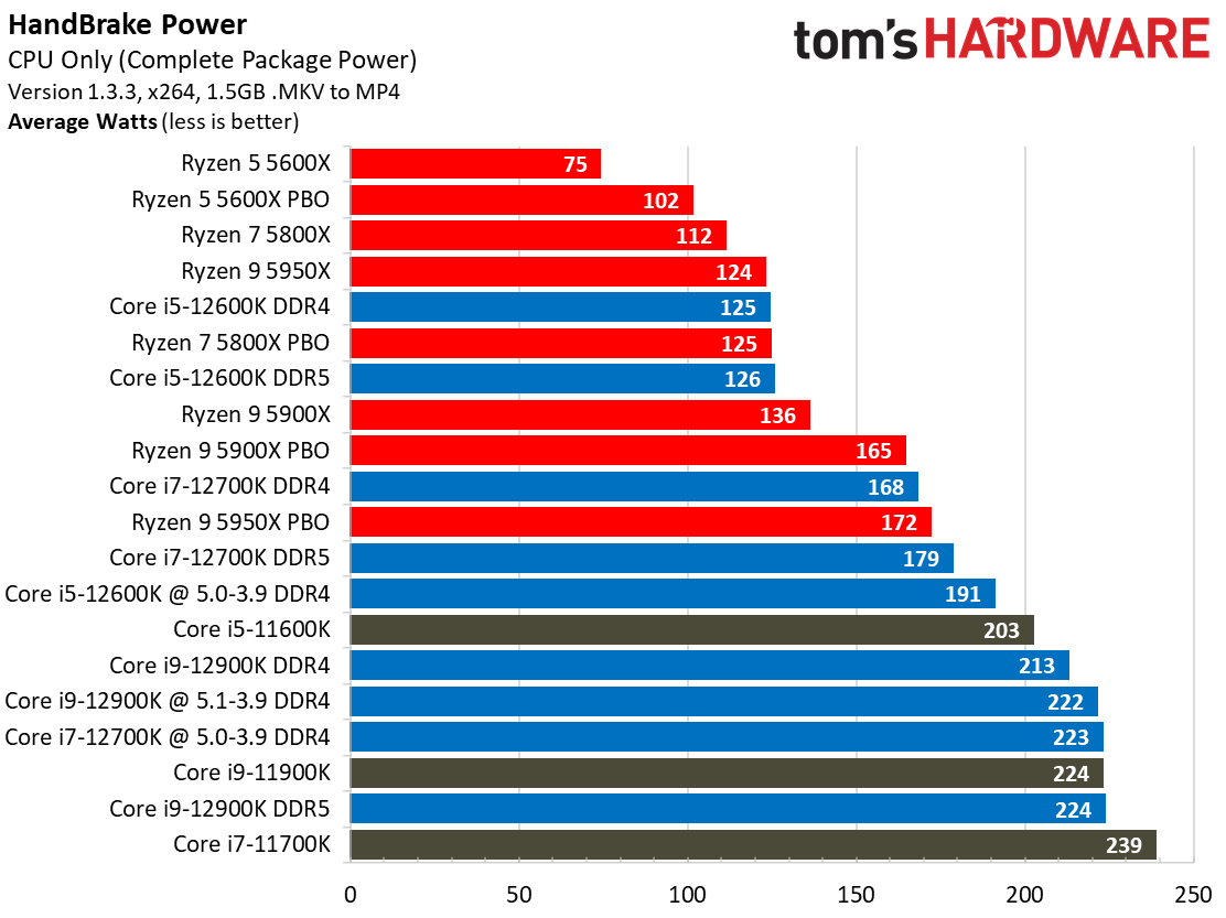
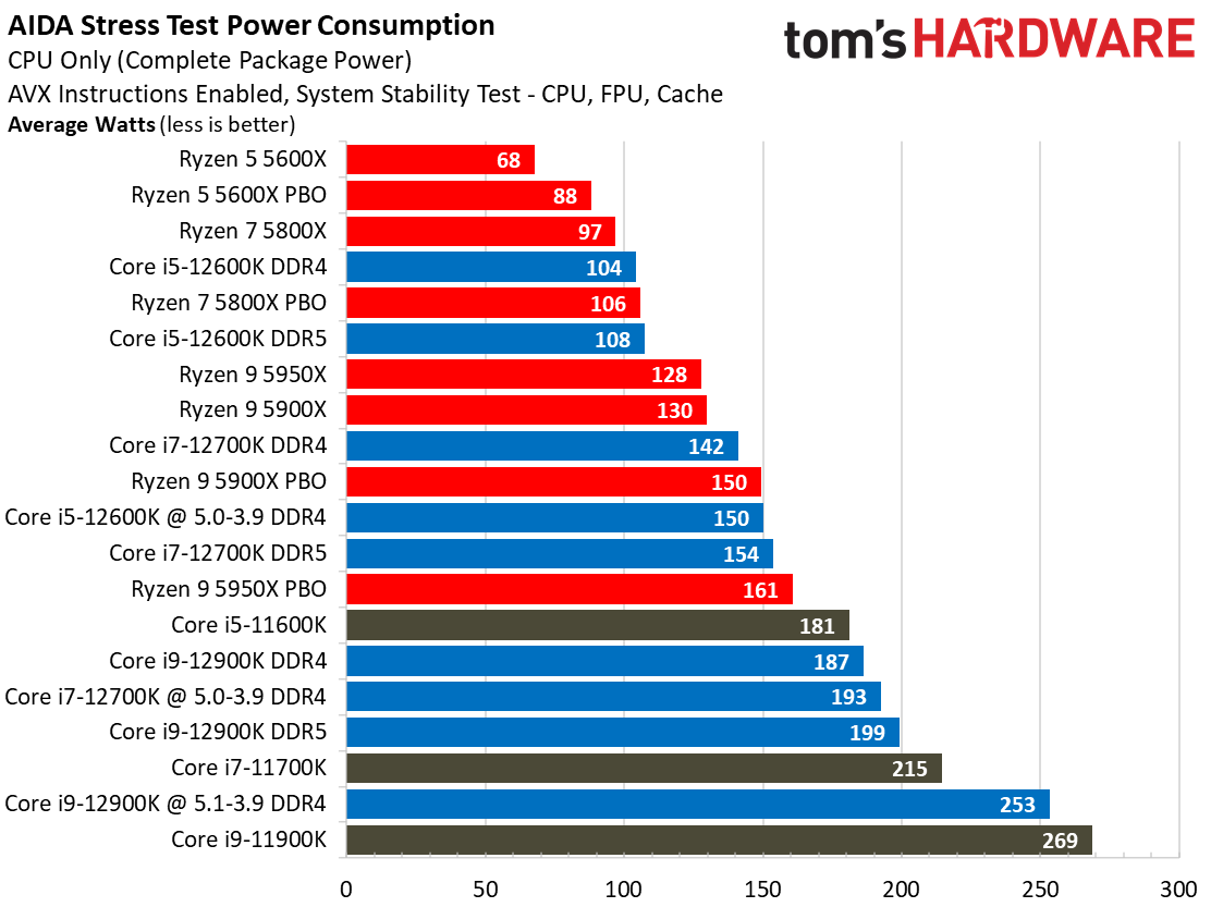
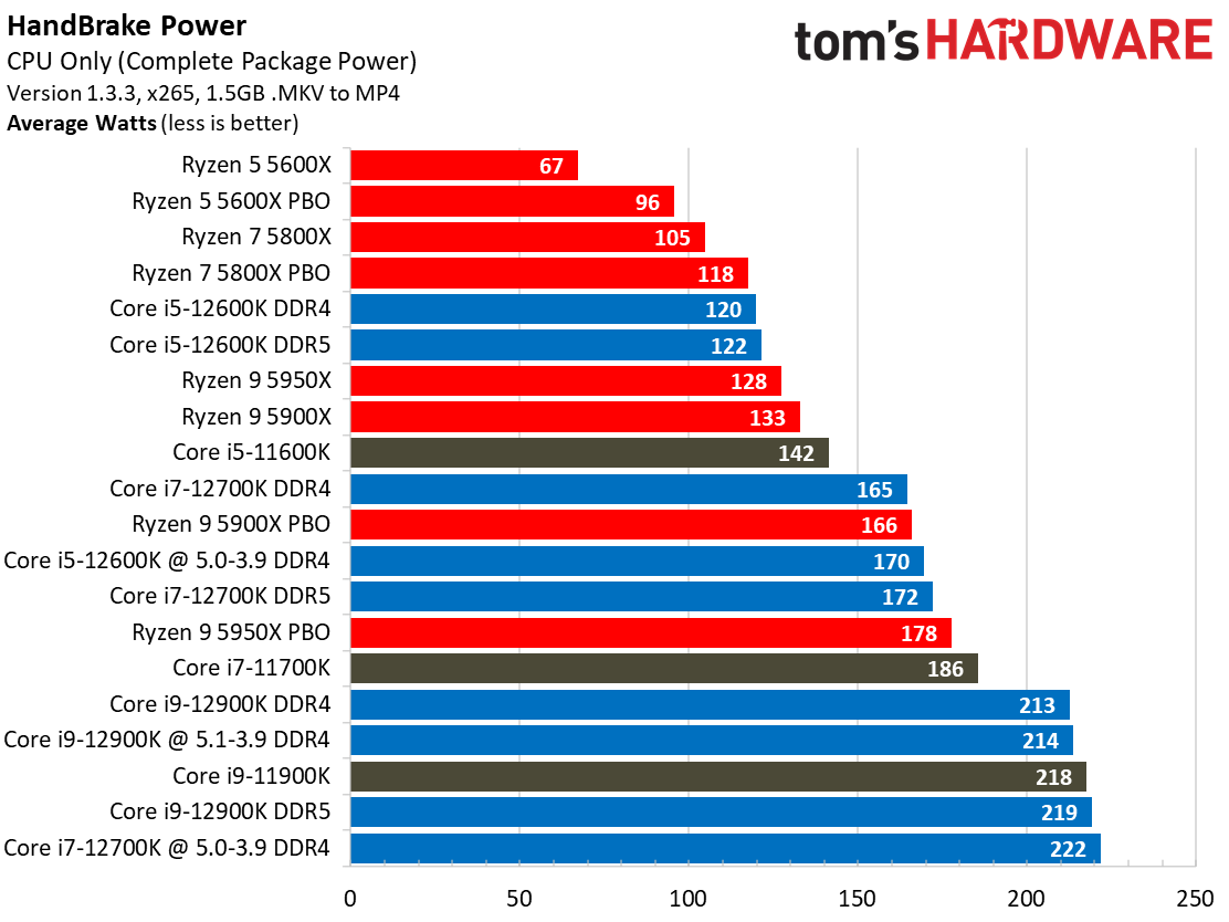
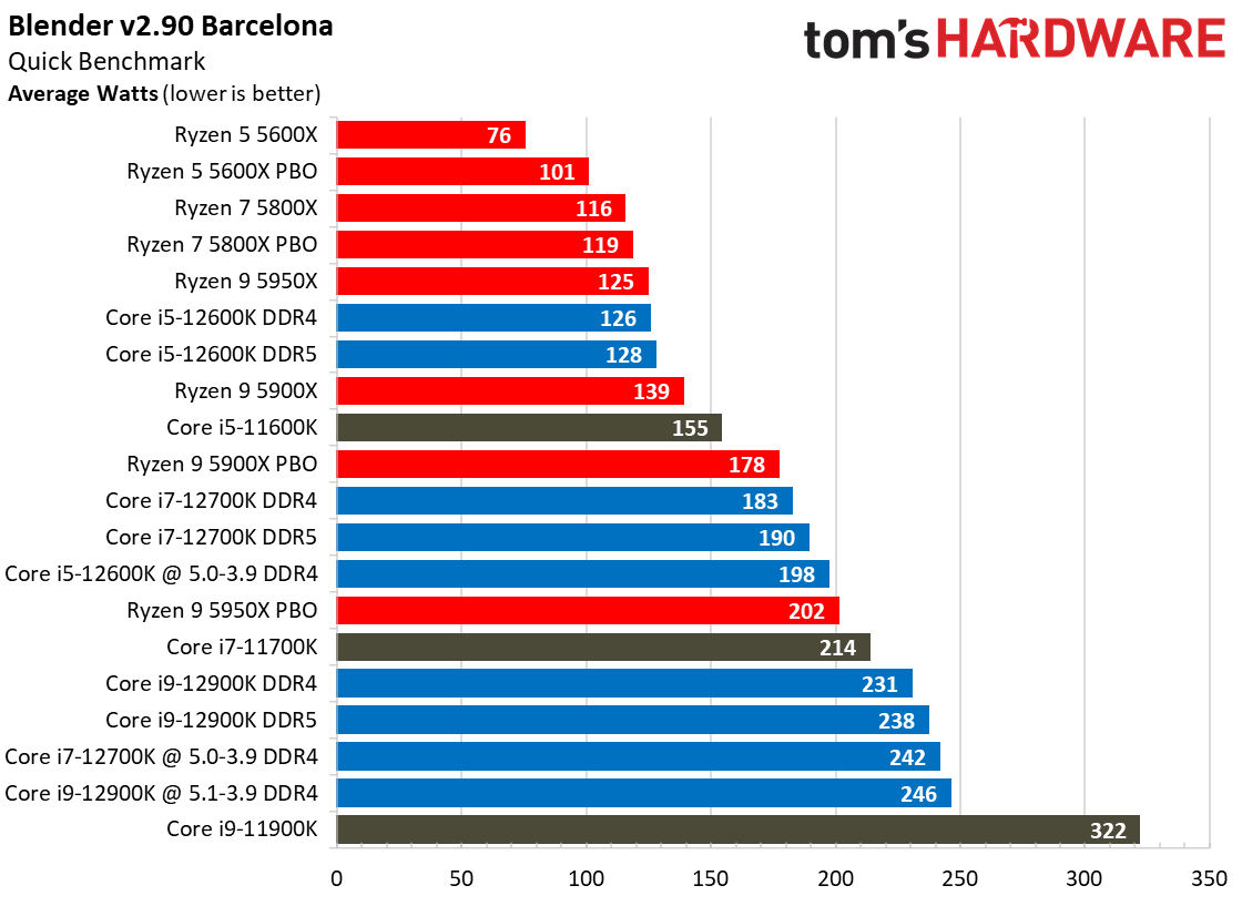
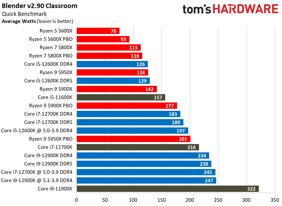
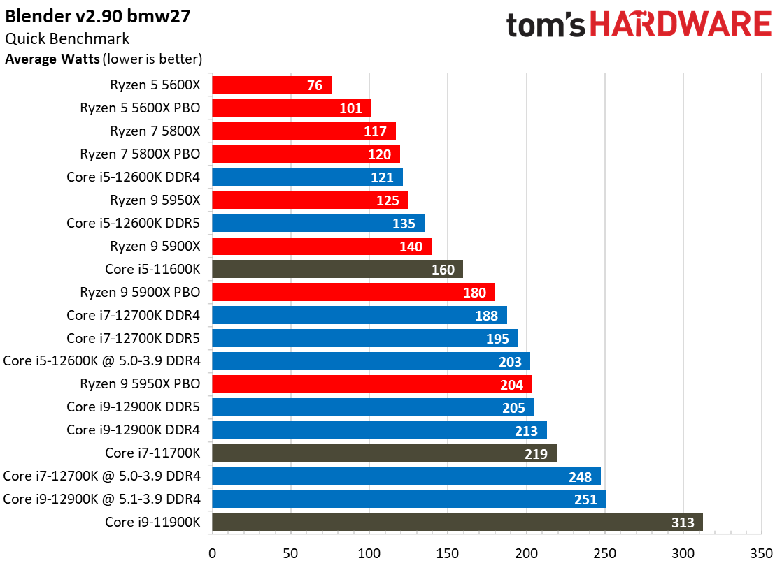
Yes, Alder Lake yet sucks more than ability than AMD'south Ryzen 5000 series chips, but the inflow of the Intel 7 procedure does mark a big comeback. As nosotros tin can see, the Alder Lake chips consume far less power than the Rocket Lake fries — we measured a peak of 238W with the 12900K, while the previous-gen 11900K drew nearly 100W more than during the same Blender workload.
Overall, Intel has reduced its power consumption from meme-worthy to an acceptable level. Likewise, Alder Lake is much faster than its predecessor, earning information technology some leeway.
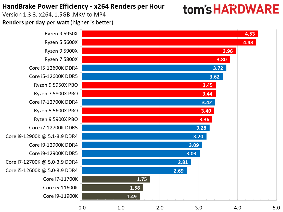
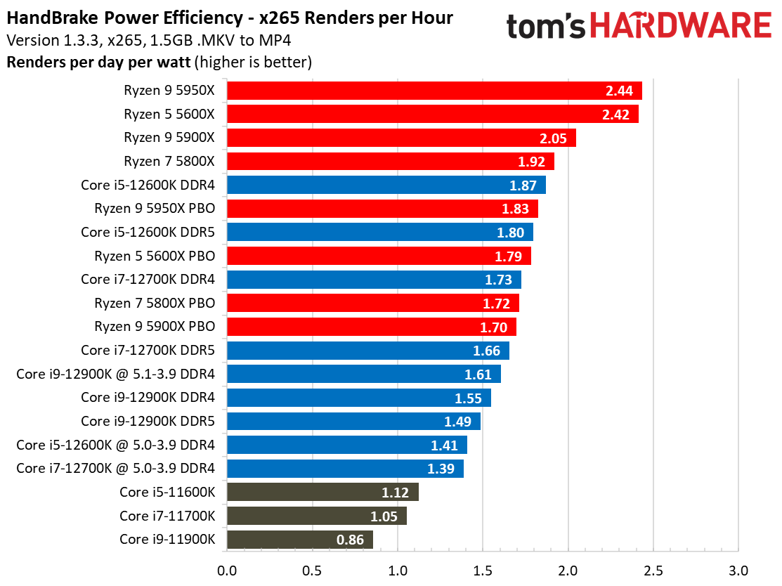
For case, as you can see in our renders-per-day measurements, the Core i9-12900K and 12600K are both twice as efficient every bit their predecessors, which is laudable. This lower power consumption results in lower cooling requirements, too.
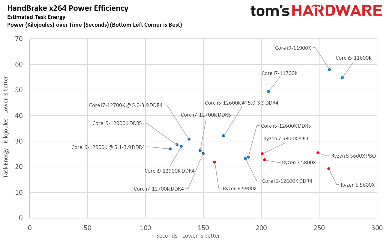
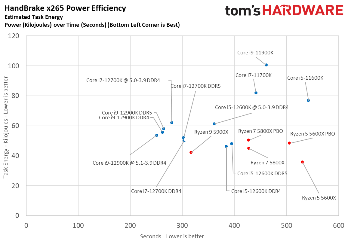
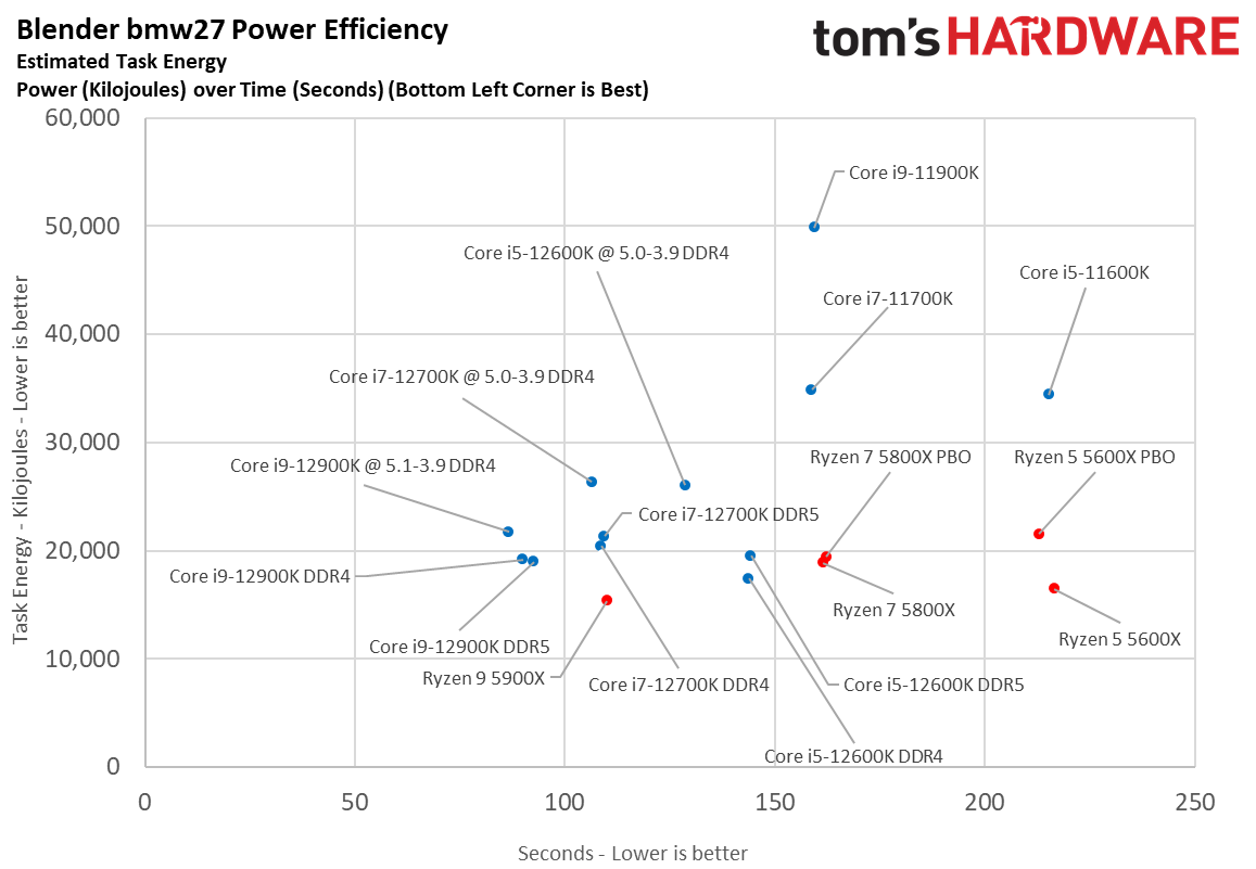
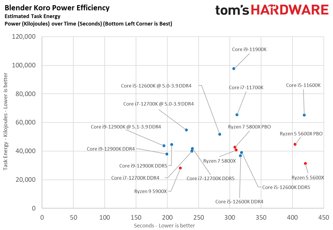
Here we take a slightly different wait at ability consumption by calculating the cumulative amount of energy required to perform Blender and x264 and x265 HandBrake workloads, respectively. We plot this 'chore free energy' value in Kilojoules on the left side of the chart.
These workloads are comprised of a fixed amount of work, so nosotros can plot the task energy confronting the time required to cease the job (bottom axis), thus generating a really useful power chart.
Bear in heed that faster compute times, and lower task energy requirements, are ideal. That means processors that fall the closest to the bottom left corner of the chart are best.
Equally you can see, Intel's chips have descended from the undesirable upper correct of the nautical chart down to the lower left manus, near matching AMD's chips in power consumption while actually being faster. That's an outstanding improvement subsequently vi years of ability-guzzling 14nm chips.
Intel Laminar Stock Coolers
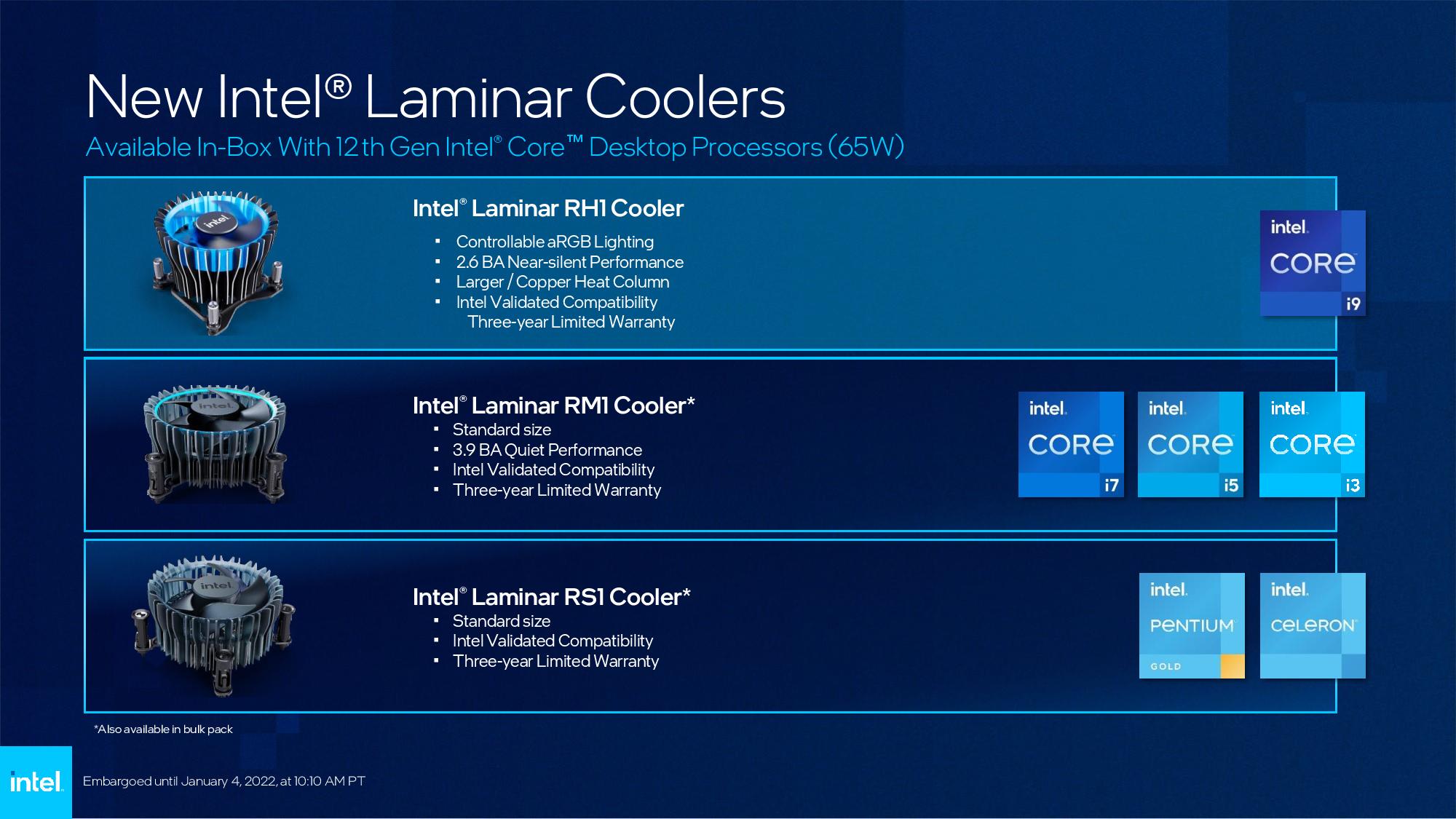
We've already seen signs of Intel's new Laminar coolers in the wild, merely at present we have the full details. These coolers are designed to address 2 major deficiencies with Intel's stock coolers: Thermal dissipation limitations and aesthetics. AMD's stock coolers have long beat Intel in both of these departments, so this is a sorely-needed upgrade.
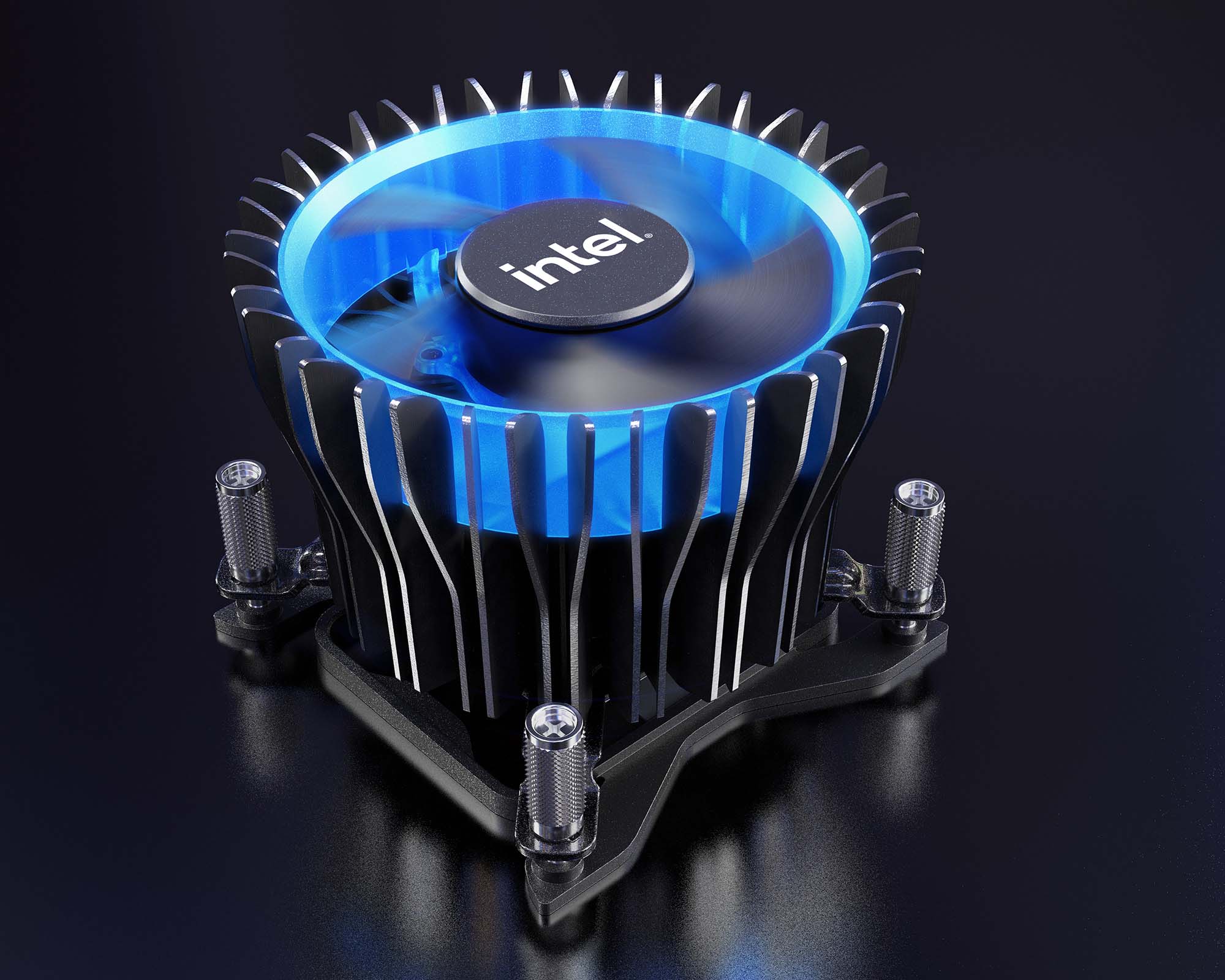
The Laminar coolers drop onto the LGA1700 socket and come up in iii variants. The Laminar RH1 has controllable aRGB lighting and features a big copper slug to amend thermal dissipation. Intel claims nearly-silent operation at two.six BA. This cooler ships with the locked Core i9 model.
The Laminar RM1 drops in for the Core i7, i5, and i3 non-Grand models and comes without RGB lighting (it does have a decorative bluish ring lining the fin stack). Intel rates this libation for 'quiet functioning' at iii.9 BA. The Laminar RS1 rounds out the new family unit of coolers, merely it's the smallest of the agglomeration and will simply ship with the lower-ability Pentium and Celeron fries. This cooler doesn't have a listed noise rating, and then you should look information technology to be fairly noisy.
Intel will also make these coolers available separate from the chips, but y'all have to buy them in lots of thou. While that puts it out of reach for nigh of usa to purchase straight from Intel, this ways that nosotros will eventually see these coolers filter out to retail outlets via third-party sellers. Nosotros're working to source these coolers for in-depth testing; stay tuned.
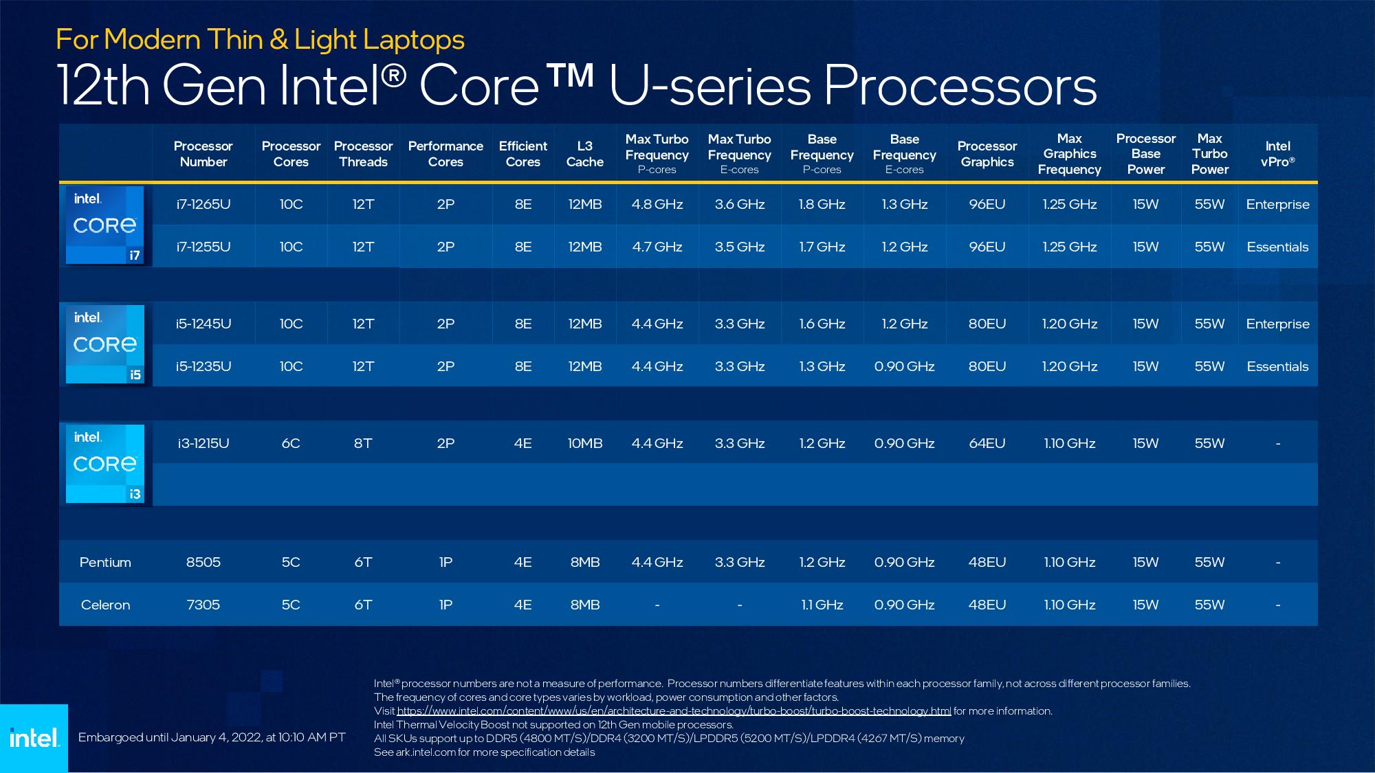
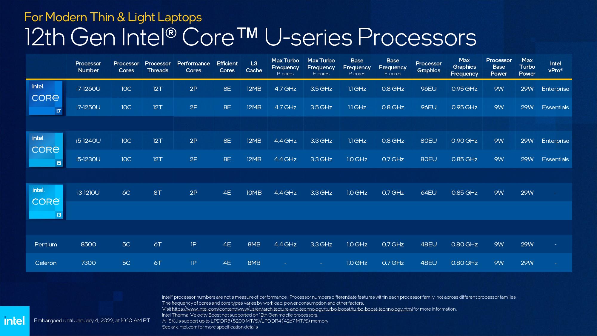
Intel Alder Lake-P and Alder Lake-Chiliad Mobile Processor Specifications
The Alder Lake mobile chips support DDR5-4800 and LPDDR5-5300, while Apple tree M1-based chips support LPDDR-6400 and AMD has LPDDR5-5500. You'll just observe the DDR5 interfaces on the higher-end Alder lake products, and back up for standard DDR5 enables end-user configurability. Intel also has options for DDR4-3200 and LRPDDR4x-4267 interfaces, which you'll notice DDR4 options on the more value-oriented platforms. All told, the Alder Lake platform supports four unlike types of memory technologies, which Intel says is a beginning for a mobile platform.
Intel also supports the PCIe five.0 interface for desktop chips simply cited both a lack of end-user devices and a lack of time to qualify the faster interface for the mobile models. As such, all of the Alder Lake mobile chips only support PCIe iv.0.
Intel's H-series lineup spans the Core i9, i7, and i5 families with a full of viii 45W SKUs designed for high-end laptops. These chips can consume up to 115W for short periods during intense work (elapsing varies based on the laptop's cooling capabilities), which will invariably impact ability consumption. Intel hasn't provided battery life projections yet (it says information technology will in the hereafter) only is frank that the Alder Lake series is tuned for performance. As such, nosotros should expect college gen-on-gen performance merely similar battery life. Intel'due south performance benchmarks beneath are impressive, but similar battery life won't practise much to accost the elephant in the room: The Apple M1-based laptops.
As you'll discover, the Alder Lake chips top out at half-dozen functioning cores while Intel'south previous-gen mobile processors had up to ten cores. Intel augments the 6 P-cores with up to eight E-cores, which allows the processor to provide similar or amend functioning in multi-threaded workloads than the previous-gen ten cadre models. Naturally, the P-cores' higher IPC also delivers more performance in single-threaded work.
The Cadre i9-12900HK is the halo scrap with vi P-cores and viii E-cores, with the former operating at up to 5.0 GHz while the latter boosts to iii.viii GHz. The P-cores feature hyperthreading, which means each host two threads, while the E-cores are unmarried-threaded. As a upshot, the Core i9-12900HK has 14 cores and 20 threads. It also comes armed with the Intel Iris Xe graphics engine with 96 EUs. (some of the i7 and i5 models have fewer EUs).
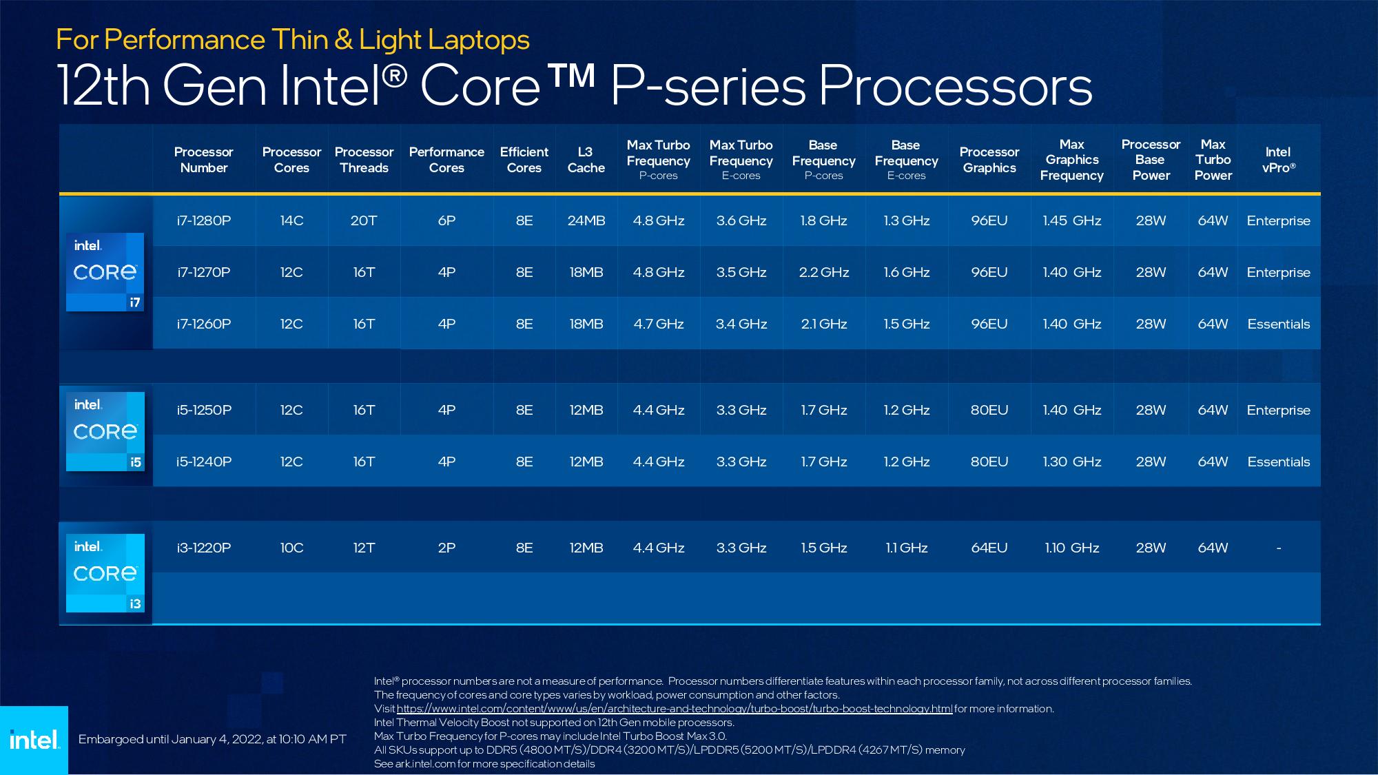
Intel also unveiled the specifications for its P- and U-series chips merely didn't provide any additional commentary. However, we can encounter that the P-serial chips have a 28W TDP and jump to a 64W TDP under load. These chips come up with either 4 or half dozen P-cores paired with eight E-cores. These chips are designed for performance thin-and-light laptops.
The U-serial is designed for thin-and-lights and supports default 9 or 15W TDPs, but can jump to 29W or 55W, which is quite the dynamic range. The U-series models come up with two P-cores and either four or viii E-cores. The U-serial drops down to 5-cadre half-dozen-thread Pentium and Celeron models, an odd organization that'due south reminiscent of Lakefield, Intel'south first hybrid bit. These U- and P-series chips will come up to market afterward in Q1, and Intel says it will share more details and so.
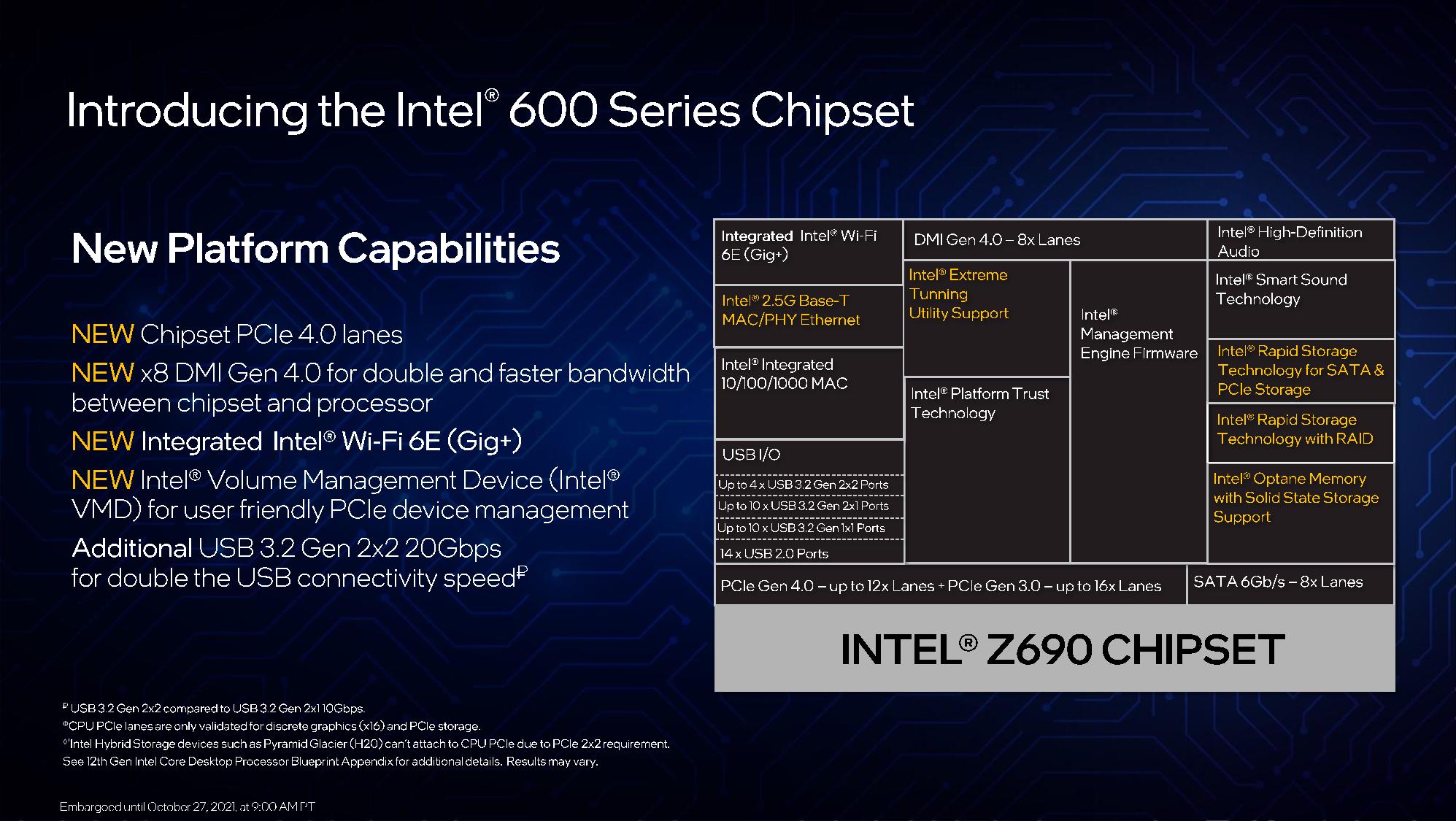
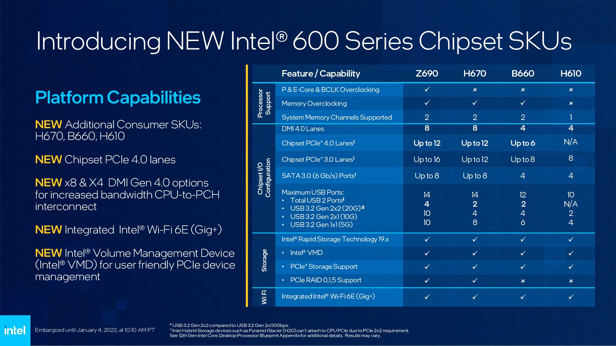
Intel Alder Lake 600-Series Motherboards, LGA1700 Socket, DDR5 and PCIe 5.0
Intel'due south ceaseless motherboard upgrades, which crave new sockets or restrict support within existing sockets, have earned the company plenty of criticism from the enthusiast customs — especially given AMD's long line of AM4-compatible processors. That trend volition go along with a new requirement for LGA1700 sockets and the 600-series chipset for Alder Lake (we've already seen enough of listings and pictures of Z690 motherboards). Still, if rumors hold truthful, Intel will stick to the new socket for at least the next generation of processors (7nm Meteor Lake) and possibly for an additional generation beyond that, rivaling AMD's AM4 longevity.
Intel also introduced its 14nm Z690 chipset for the initial release, and you can read virtually the chipset and some of the first 60+ motherboards in our Z690 motherboard roundup here. There'due south a wide choice of DDR5 motherboards spread amongst the various motherboard makers' loftier- and lower-end Z690 families. Notwithstanding, DDR4 models appear to be bars to the lower-cease Z690 boards (dissimilar previous generations, no motherboard supports both DDR4 and DDR5). We look pricing for DDR5 to be substantially higher than DDR4, currently projected to be a 50 to threescore% markup, for some fourth dimension.
Z690 motherboards are more than expensive than lower-end alternatives, merely we expect the lower-stop Alder Lake H670, B660 and H610 motherboards to be announced at CES 2022.
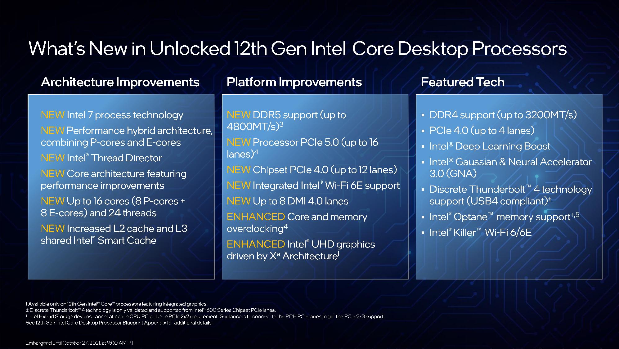
Alder Lake supports upwardly to 16 lanes of PCIe 5.0 (technically for storage and graphics only, no networking devices) and an additional 4 lanes of PCIe 4.0 from the chip for Thou.2 storage. Intel has too added 12 lanes of PCIe 4.0 that hang off the chipset, a nice step upwardly from the Z590 chipset's PCIe iii.0 support. That provides a total of 28 PCIe platform lanes for Alder Lake systems. Intel as well doubled the throughput of the DMI connection between the flake and chipset from an x8 DMI 3.0 pipe, which clocks in at vii.88 GB/s, to an x8 DMI 4.0 connection that delivers 15.66 GB/s. Intel too added support for the Volume Management Device characteristic that enables PCIe SSD direction and the ability to create bootable RAID configurations.
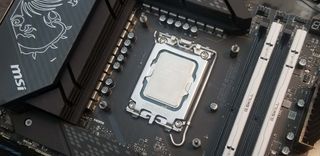
Because the LGA1700 socket is bigger than the electric current sockets used in LGA1151/LGA1200 motherboards, existing coolers may be incompatible, simply cooler conversion kits, which almost cooler makers volition provide for free for existing customers, tin can conform the larger socket. (Coolers that support both LGA11xx and LGA2066 already be, so an in-between pick isn't as well difficult.)
The larger socket is needed to accommodate 500 more than pins than the LGA1200 socket. Those pins are needed to back up newer interfaces, like PCIe 5.0 and DDR5, among other purposes, like ability commitment. Intel has as well listed Alder Lake-S BGA back up documentation, indicating that soldered-down models will also come to market.
PCIe 5.0 and DDR5 support give Intel a connectivity advantage over competing chips, but there are a lot of considerations involved with these big engineering transitions. Equally nosotros saw with the motility from PCIe 3.0 to 4.0, a step up to a faster PCIe interface requires thicker motherboards (more layers) to accommodate wider lane spacing, more robust materials, and retimers due to stricter trace length requirements. All of these factors conspire to increase cost.
Nosotros can look those same PCIe 4.0 requirements to become more than arduous for motherboards with a PCIe 5.0 interface, particularly because they will crave retimers for even shorter lane lengths and fifty-fifty thicker motherboards. That means we could meet yet another jump in motherboard pricing over what the industry already absorbed with the motility to PCIe iv.0. Additionally, PCIe 5.0 likewise consumes more ability, which volition present challenges in mobile form factors.
Intel has appear that Alder Lake will support DDR5 retention, but that volition crusade pricing pressure level. Notably, every transition to a newer retentiveness interface has resulted in college up-forepart DIMM pricing, which is concerning in the price-sensitive desktop PC market. DDR4 for example first came to the HEDT segment on Intel's X99 platform in 2014, and pricing at the time was more than double the cost of DDR3. Skylake brought DDR4 to the mainstream segment in 2015, but information technology still carried a 25-50% toll premium. Electric current signs point to a l% to threescore% premium for DDR5 retentiveness.
DDR5 is in the opening stages; some vendors, like Adata, TeamGroup, and Micron, have already begun shipping modules. The inaugural modules are expected to run in the DDR5-4800 to DDR5-6400 range. The JEDEC spec tops out at DDR5-8400, but every bit with DDR4, it will take some time before we see those pinnacle speeds.
We have, all the same, seen signs that but the higher-cease Alder Lake desktop PC platforms, similar Z-series motherboard, will support DDR5, while lower-end boards volition use DDR4 for a friendlier cost of entry.
Intel'due south pricing model with the Alder Lake chips is vicious — based on their performance, every model undercuts competing Ryzen 5000 fries past large margins. That ways the Alder Lake chips are a great value, but the loftier pricing associated with the expensive Z690 motherboards has been a hurting signal that, in some cases, allows AMD to remain competitive on overall platform costs. Those high prices tend to stem primarily from support for DDR5 and the PCIe 5.0 interface. The DDR5 shortages, and resulting price scalping, certainly haven't helped matters, either. Unfortunately, there are precious few loftier-terminate DDR4 Z690 options available.
Intel plans to accost the loftier motherboard pricing consequence with the H670, B600, and H610 chipsets. We're told that we should wait the new motherboards with these chipsets to predominantly support lower-price DDR4 memory.
Notably, retention overclocking is allowed with all Alder Lake processors, including locked models, on the B660 and H470 platforms. We have a much deeper breakup of the new chipset features and a roundup of the motherboards nosotros know about here, so caput there for more than detail.
Intel Alder Lake: TDP vs PBP and MTP
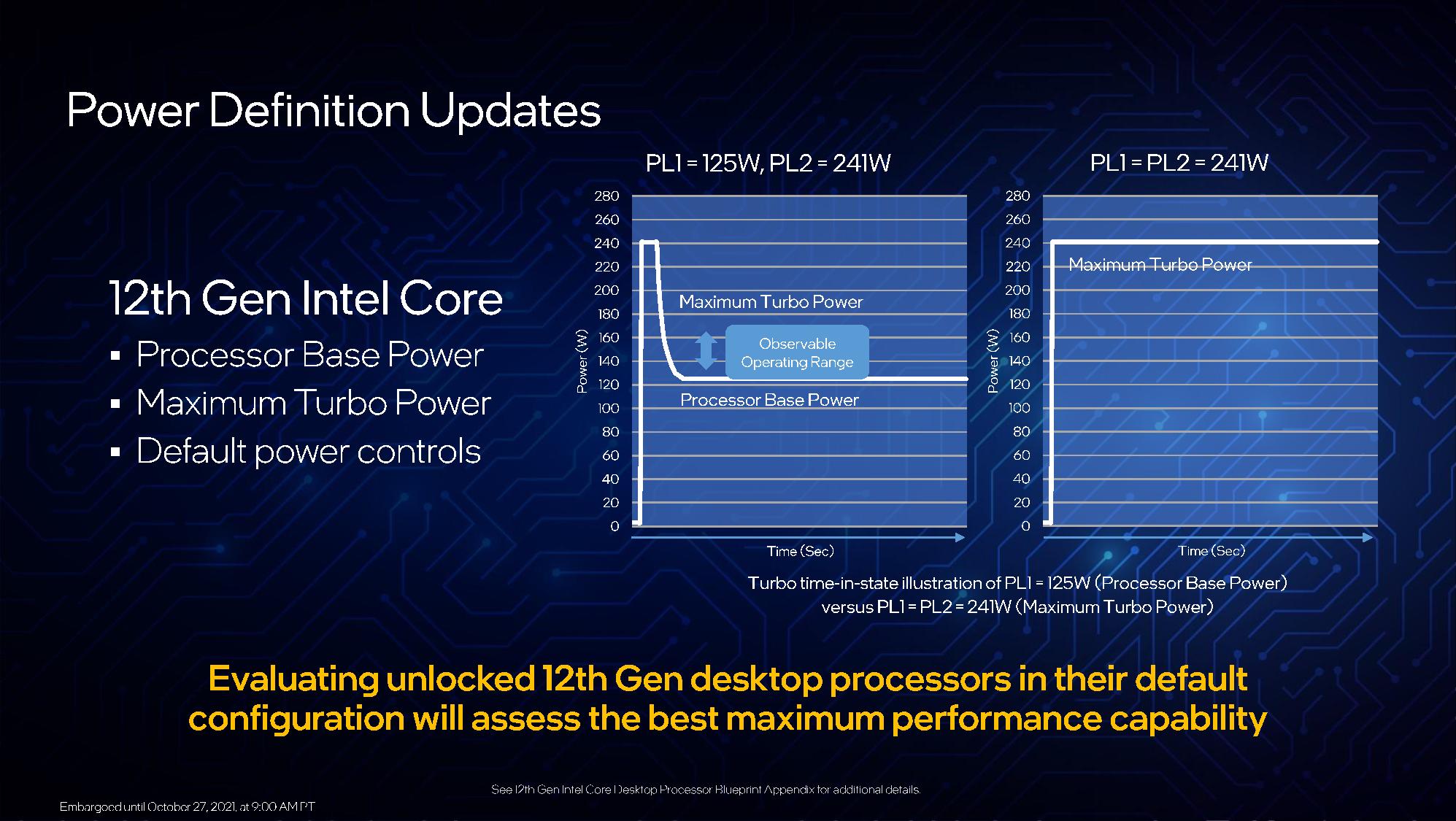
Intel has long listed the TDP of a processor every bit its guaranteed rating at base frequencies, also known as PL1. Nonetheless, the fleck tin can besides opportunistically (meaning this isn't guaranteed) boost to higher frequencies and thus eat far more power, but just if it is safely within certain power, temperature, and electric current limits. This is called the PL2 power state, and Intel hasn't included this metric on its standard spec sheets.
Now Intel has redefined its power nomenclature to accept a 'Processor Boost Ability' (PBP) value representing the guaranteed base operation level (PL1). This replaces TDP. Intel will besides now listing a 'Maximum Turbo Power' (MTP) specification that quantifies the power consumption during Turbo Heave, besides known as PL2. That means yous'll no longer encounter a TDP rating on the spec sheet.
Intel's processors have a 'Tau Duration' setting that dictates how long the processor can stay in the boosted MTP state (PL2) before it drops back downwards to the PBP state (PL1 – base power). Intel specified this elapsing as 58 seconds for Rocket Lake fries, simply this is but a guideline. Motherboard vendors are gratuitous to change this value to any length of fourth dimension if their motherboard can handle the power commitment required to sustain the boost. Every bit shown in the graphic above, most motherboard vendors alter the Tau setting to infinite to stay within boost for an infinite amount of time. Given that Intel'due south Tau settings are only recommendations, the chip remains inside of the warranty regardless of boost duration. Every bit an space Taue is a common practice on most every enthusiast motherboard, Intel will at present set the Tau to a default of 'infinite' for all of its K-serial (overclockable) models, but retain the same 58-second duration for its locked chips. This means that the Core i9-12900K's MTP (PL2) is now the same equally its PBP (PL1). In other words, the fleck will e'er operate at 241W.
Additionally, the new desktop PC motherboards for Alder Lake chips will herald the inflow of mainstream ATX12VO motherboards that leverage a new lower-ability PSU specification. Both systems with support for standard power supplies and the ATX12VO spec are planned, merely Intel is on a total-court press to push the adoption of the new standard. However, despite Intel's fondness for the standard, nosotros have yet to see a significant number of 600-serial boards that support ATX12VO. Nearly all boards work with standard power supplies.
Intel twelfth-Gen Alder Lake Xe LP Integrated Graphics
The media engine, in this instance the aforementioned Gen12 Xe LP architecture constitute in Tiger Lake simply ported to the Intel 7 process, comes in two variants: one with 32 EUs (GT1) for desktop PCs, and another GT2 variant with 96 EUs for the mobile variants. The desktop PC models come with 33% more than EUs than the current desktop fries with Gen9.five UHD 630 Graphics, but that'southward a far weep from the 96 EUs constitute in 11th Gen Tiger Lake. Only this is on the desktop, where nearly users that care about graphics performance will simply utilize a dedicated GPU.
Intel says the Xe LP engine supports 1080p gameplay and features a 12-fleck finish-to-end video pipeline. The desktop PC models don't have Thunderbolt 4 connectivity or an prototype processing unit (IPU), with those features being used only for mobile variants.
The UHD 770 engine clocks in at (upwards to) 1550, 1500, and 1450 MHz for the 12900K, 12700K, and 12600K, respectively.
We've also seen Alder Lake-P benchmarks (the mobile chips) with the GT2 configuration, with 96 EUs (768 shaders). The early Xe LP iGPU silicon on the -P model runs at 1.15GHz, but as with all engineering samples, that could change with shipping models.
Alder Lake's integrated GPUs back up upward to 5 brandish outputs (eDP, dual HDMI, and Dual DP++), and support the same encoding/decoding features as both Rocket Lake and Tiger Lake, including AV1 8-bit and x-chip decode, 12-flake VP9, and 12-bit HEVC.
Intel Alder Lake CPU Architecture
Intel pioneered the x86 hybrid architecture with its Lakefield fries, with those inaugural models coming with ane Sunny Cove cadre paired with four Atom Tremont cores.
Compared to Lakefield, both the high- and low-performance Alder Lake-Southward cores take a pace forwards to newer microarchitectures. Alder Lake-S actually jumps forwards 2 'Cove' generations compared to the 'big' Sunny Cove cores found in Lakefield. The big Golden Cove cores come with increased single-threaded operation, AI performance, Network and 5G performance, and improved security features compared to the Willow Cove cores that debuted with Tiger Lake.

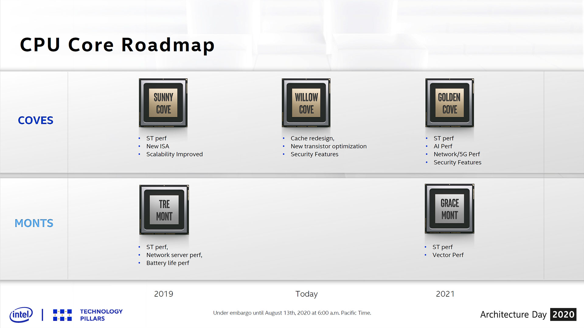
Alder Lake's smaller Gracemont cores jump forward a unmarried Atom generation and offering the benefit of being more power and area efficient (perf/mm^ii) than the larger Gilded Cove cores. Gracemont also comes with increased vector performance, a nod to an obvious improver of some level of AVX back up (probable AVX2). Intel also lists improved single-threaded performance for the Gracemont cores.
You tin can read our deep-dive coverage of the Golden Cove Operation Core architecture hither. In summary, the Golden Cove microarchitecture is designed for low-latency single-threaded performance and comes with an average of xix% more than IPC than the Cypress Cove architecture in Rocket Lake. It also supports AVX-512 and AMX (a new AI-focused matrix-multiply ISA) for data center variants (both are disabled on consumer chips).
You can likewise read our deep dive coverage of the Gracemont Efficiency Core compages here. In summary, the single-threaded Efficiency (E) core, which comes with the Gracemont microarchitecture, is designed to improve multi-threaded performance and provide infrequent expanse efficiency (small footprint) and performance-per-watt. Four of these pocket-size cores fit in the same area as a Skylake core and deliver lxxx% more than performance in threaded piece of work (at the same power). A unmarried E core also delivers 40% more functioning than a single-threaded Skylake cadre (at the same ability) in single-threaded work (caveats utilise to both).
Lakefield served as a proving ground not only for Intel's 3D Foveros packaging tech but besides for the software and operating organisation ecosystem. At its Architecture Day 2020, Intel outlined the performance gains to a higher place for the Lakefield chips to highlight the promise of hybrid designs. Still, the results come with an important caveat: These types of operation improvements are simply available through both hardware and operating system optimizations. Let's look at Intel's solution to that problem.
Intel Thread Manager
Intel unveiled the answer to the software challenge at its Architecture Day 2021 — the new Thread Manager. Due to Alder's apply of both faster and slower cores that are optimized for different voltage/frequency profiles, unlocking the maximum performance and efficiency requires the operating organisation and applications to accept an sensation of the fleck topology to ensure workloads (threads) state in the correct core based on the type of application.
The electric current thread scheduling systems are based entirely on static rules (priority, foreground, background) and tend to be inefficient and create software programming overhead. That'due south where Intel's Thread Managing director technology comes in. This hardware-based technology provides enhanced telemetry information to Windows 11 to assure that threads are scheduled to either the P or E cores in an optimized and intelligent manner, but in a way that's transparent to software.
This engineering science works by feeding the Windows eleven operating system with low-level telemetry data collected from within the processor itself, thus informing the scheduler about the state of the cadre, be it power, thermal or otherwise. (As we covered here, Intel has integrated a new power microcontroller in each Gracemont core, a first, that collects similar data on the society of microseconds instead of milliseconds, and so it might exist role of the new telemetry system.)
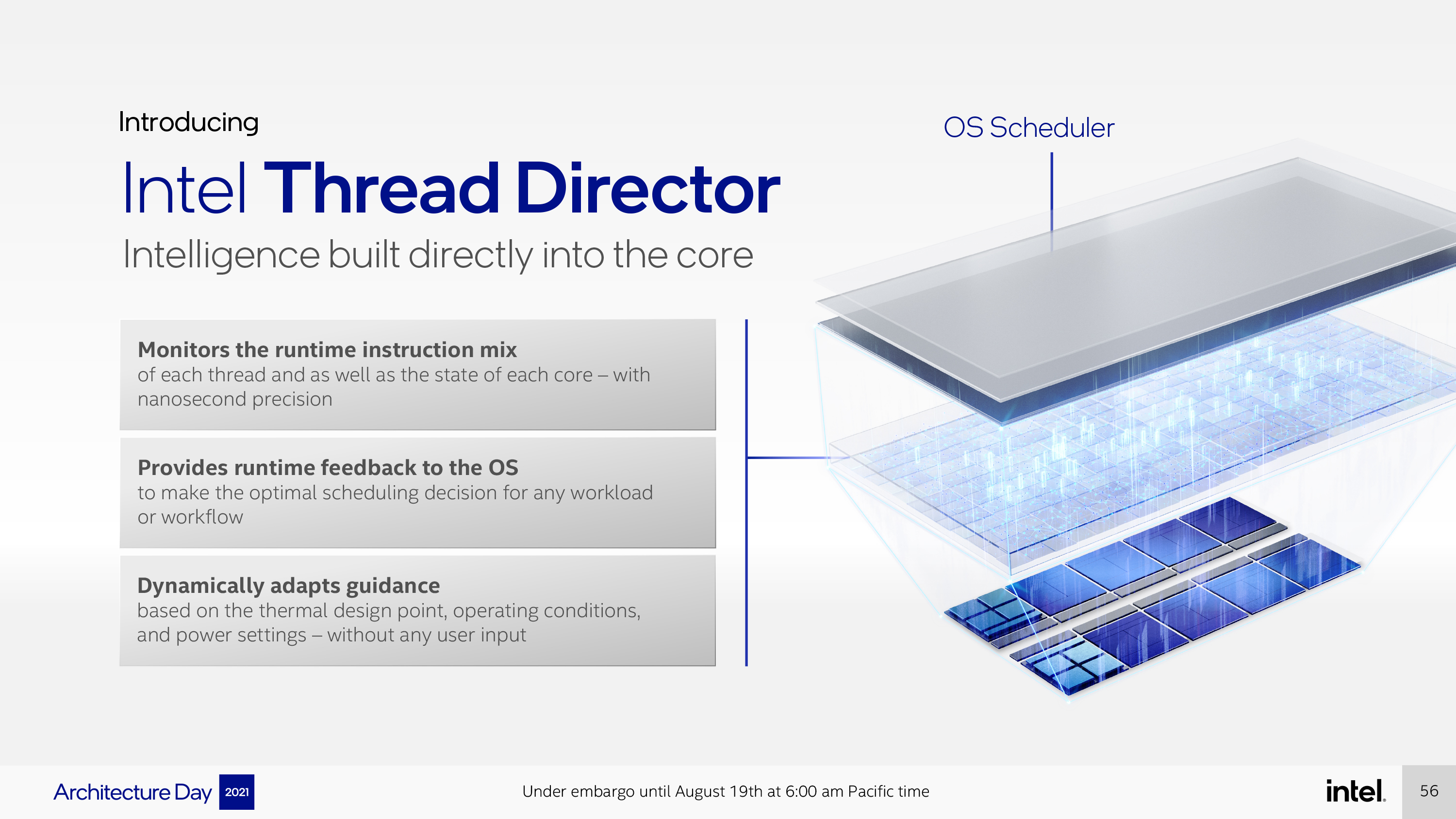
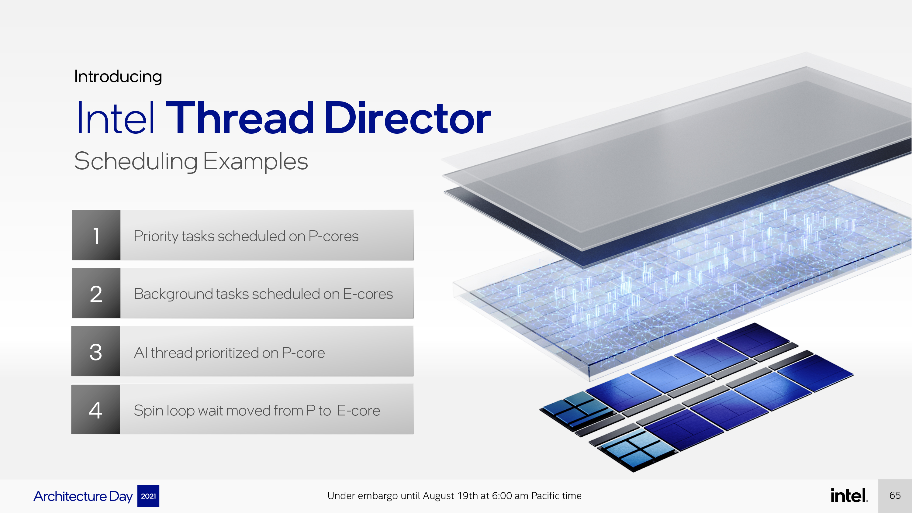
Additionally, Thread Manager can also notice the instruction mix (scalar/vector) used in any given thread at a nanosecond granularity, and so communicate with the Windows 11 scheduler to steer the thread to the right execution core, be that a high-performance P-Core or an efficient E-Core. Typically, vector/AI workloads will exist prioritized to performance cores while scalar instructions and background tasks are moved to efficiency cores. However, the system is dynamic, so thread placement decisions can vary based on the dynamic mix of conditions and workloads present on the processor at whatsoever given time.
Additionally, threads can go through various phases and instruction mixes over their lifetime, so the scheduler constantly re-adjusts based on the real-time telemetry data. This is helpful when the number of threads designated for 'functioning' outnumber the available cores, for case. In that case, less enervating 'operation' threads, such equally a plan in a spin loop, can exist moved off to the efficiency cores while more deserving workloads are assigned to the operation cadre.
Previously, the operating organisation didn't take access to this type of telemetry data to inform scheduling decisions, instead using simple data like whether the process was a foreground or background job. This enhanced organization allows the operating system and processor to work in tandem to assure right scheduling in real-fourth dimension, thus fugitive costly software re-coding. This is a promising sign that existing lawmaking volition run well on the Alder Lake processors.
Programmers tin access more granular command, likewise, by specifying that certain threads are used in a sure mode through an expansion of the PowerThrottling API that allows developers to assign a QoS attribute to their threads. Additionally, a new EcoQos classification lets software tag threads that reply best on the efficiency cores to assure they are prioritized to execute on the E-Cores. Microsoft says that the Edge browser and 'various' Windows 11 components now have advantage of the EcoQos classification system, and we can expect back up to broaden quickly.
This looks to be a promising and less-intrusive (at to the lowest degree from a coding standpoint) method of ensuring that the correct threads land on the correct cores, thus delivering optimal performance. That said, nosotros'll have to see it in activeness before we can pass judgement on its efficacy – much of its potency will boil down to the latency involved with the process of communicating telemetry data and moving the thread, and intel isn't sharing those details yet. Additionally, it's possible that an backlog of communication between the Thread Managing director and the Windows 11 scheduler could create a challenging workload of its ain, and then finding the right corporeality of granularity volition be fundamental to assuring both timely thread placement and a minimum of organisation overhead.
The system is already far in development, and Microsoft says that further enhancements to the engine are already underway and in planning for Windows 11, with more details to be shared at a later date.
Alder Lake chips will also piece of work fine with a bog-standard Windows ten operating organization – existing thread-scheduling techniques go on to work with the processors, just not also. While the chips work, you'll miss out on the enhanced capabilities of Thread Director (that's Windows eleven only), which will have a varying affect on operation and power consumption based on education type and awarding usage models. In other words, your mileage will vary.
The hybrid architecture could however consequence in some teething pains, equally Intel itself recently divulged that some older games with DRM might not piece of work with the new chips unless developers add specific software optimizations.
Finally, it has long been known that the Gracemont cores do non back up the AVX-512 instruction prepare, and speculation has been rife about how the lawmaking would work on Alder Lake processors, if at all. Intel'south answer is uncomplicated: AVX-512 will not piece of work on either type of cadre nowadays in Alder Lake. The loftier-performance cores do characteristic the Golden Cove architecture that supports AVX-512 natively, simply Intel has fused that feature off (aye, the 512-bit FMA is still present and consumes die area) for the consumer fries. In contrast, server fries with Golden Cove accept ii 512-bit FMAs and fully support AVX-512. Meanwhile, the Gracemont cores are simply non AVX-512 capable, and disabling support allows the Alder Lake chip to have uniform ISA support.
Information technology is completely clear that the AMD vs Intel boxing has been reignited. Head to our Intel Core i9-12900K and Core i5-12600K review for additional in-depth testing and ownership advice.
championrestargem1966.blogspot.com
Source: https://www.tomshardware.com/news/intel-alder-lake-specifications-price-benchmarks-release-date
0 Response to "How Read Engine Codes 2002 Ultra Classic"
Post a Comment